Driver circuit for switching edge modulation of a power switch
- Summary
- Abstract
- Description
- Claims
- Application Information
AI Technical Summary
Benefits of technology
Problems solved by technology
Method used
Image
Examples
Embodiment Construction
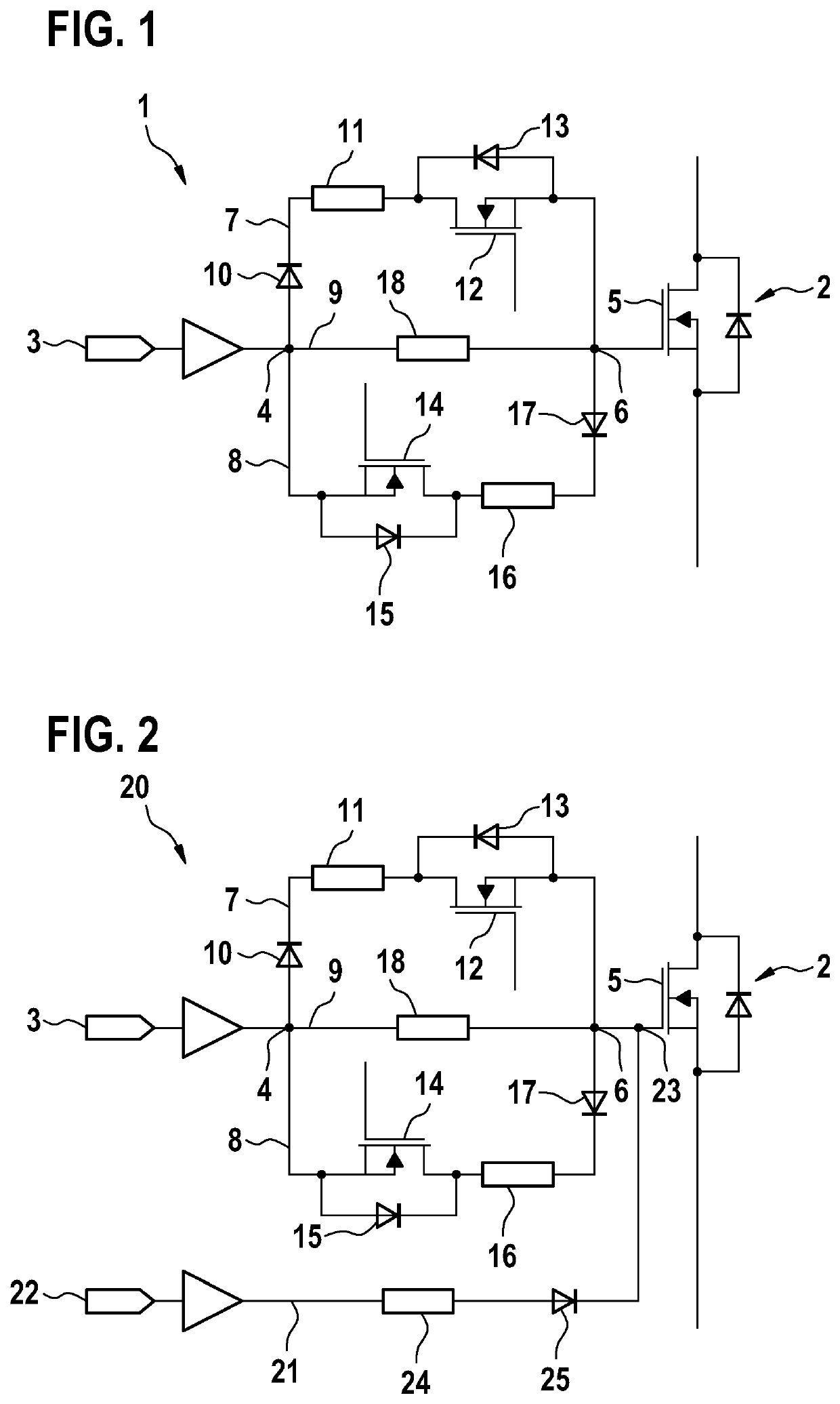
[0039]FIG. 1 shows a circuit diagram of a first specific embodiment of a driver circuit 1 according to the present invention of a power switch 2. Driver circuit 1 includes a first driver circuit input 3 including a downstream input node 4. Driver circuit 1 furthermore includes a power switch transistor 5 including an upstream first gate node 6.
[0040]A charging path 7, a discharging path 8, and a gate path 9 are situated between input node 4 and first gate node 6. A gate of power switch transistor 5 of power switch 2 is connected to first gate node 6. Driver circuit 1 is configured in such a way that, during a switching process of power switch 2, gate path 9 is temporarily short-circuited either via charging path 7 or discharging path 8, to increase the slope of the switching behavior of power switch 2. Charging path 7 and discharging path 8 are blocked at the beginning and end of a switching process for overvoltage reduction.
[0041]Starting at input node 4, the following components a...
PUM
 Abstract
Description
Claims
Application Information

