Output circuit for semiconductor device, semiconductor device having output circuit, and method of adjusting characteristics of output circuit

a technology of output circuit and output buffer, which is applied in the direction of impedence matching network, measurement device, static storage, etc., can solve the problems of reducing the time required for calibration operation, affecting the precision of output buffer impedance, and requiring different impedances from the time of data output, so as to reduce the time necessary for calibration operation and reduce the circuit scale of the calibration circuit

Active Publication Date: 2006-07-20
LONGITUDE LICENSING LTD
View PDF10 Cites 64 Cited by
  • Summary
  • Abstract
  • Description
  • Claims
  • Application Information

AI Technical Summary

Benefits of technology

[0009] It is another object of the invention to decrease the calibration time.
[0013] According to the present invention, the impedances of the first and the second output buffers can be set in common based on the calibration operation. Therefore, the calibration circuit that is used to adjust the impedance at the data output time and the calibration circuit that is used to adjust the impedance at the ODT operation time do not need to be provided separately. Consequently, the circuit scale of the calibration circuit can be decreased.
[0014] Because the impedance adjustment at the data output time and the impedance adjustment at the ODT operation time can be completed simultaneously in one-time calibration operation, time necessary for the calibration operation can be decreased.

Problems solved by technology

When the amplitude of the input and output signals is made smaller, the required precision of the impedance of the output buffer becomes considerably severe.
In addition, the impedance is also affected by a change in the ambient temperature and a variation in power supply voltage during the actual usage of the semiconductor device.
However, usually, during the ODT operation, impedance which is different from that during the data output time is required.
This has a problem in that the circuit scale becomes large.
Therefore, there is a problem in that it takes time for the calibration.
However, when the calibration is carried out periodically during the actual use time, this problem becomes serious.

Method used


Image

  • Output circuit for semiconductor device, semiconductor device having output circuit, and method of adjusting characteristics of output circuit
  • Output circuit for semiconductor device, semiconductor device having output circuit, and method of adjusting characteristics of output circuit
  • Output circuit for semiconductor device, semiconductor device having output circuit, and method of adjusting characteristics of output circuit

Examples


Embodiment Construction

[0027] Preferred embodiments of the present invention will now be explained in detail with reference to the drawings.

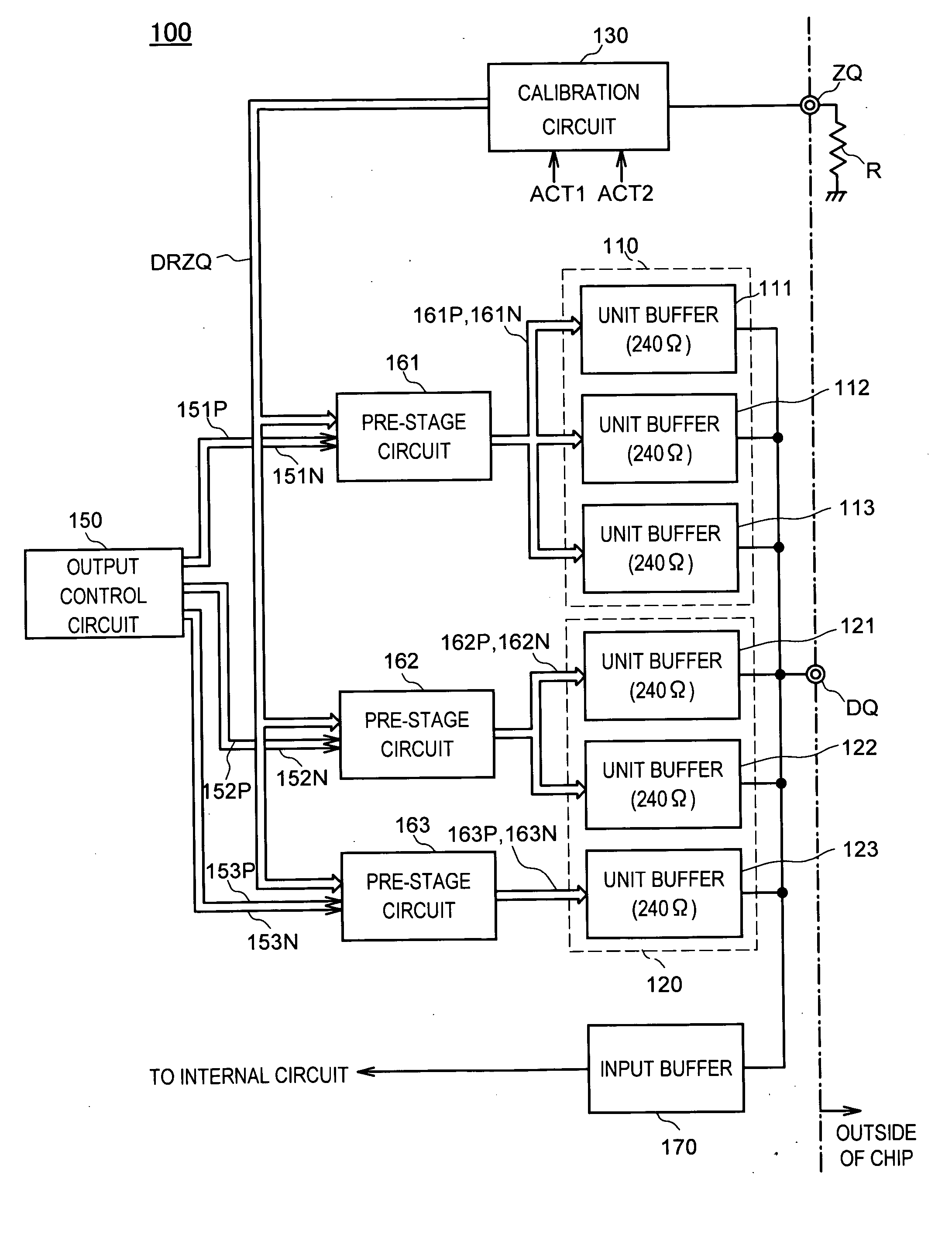
[0028]FIG. 1 is a block diagram of a configuration of an output circuit (an input and output circuit) 100 of a semiconductor device according to a preferred embodiment of the present invention.

[0029] As shown in FIG. 1, the output circuit 100 according to the present embodiment includes a first output buffer 110 and a second output buffer 120 that are connected to a data pin DQ, a calibration circuit 130 that is connected to a calibration pin ZQ, and an input buffer 170 that is connected to the data pin DQ.

[0030] The output circuit (the input and output circuit) 100 according to this embodiment has the ODT function in addition to the ordinary data input and output function. The ODT function is the function of preventing a reflection of a signal, by making the output circuit function as a terminal resistor, when other semiconductor device is carrying out a data tran...


PUM


Abstract

To decrease the circuit scale necessary for the calibration of the output circuit and to decrease the time required for the calibration operation. The invention includes a first output buffer and a second output buffer that are connected to a data pin, and a calibration circuit that is connected to a calibration pin. The first output buffer and the second output buffer include plural unit buffers. The unit buffers have mutually the same circuit structures. With this arrangement, the impedances of the first output buffer and the second output buffer can be set in common, based on the calibration operation using the calibration circuit. Consequently, both the circuit scale necessary for the calibration operation and the time required for the calibration operation can be decreased.

Description

TECHNICAL FIELD [0001] The present invention relates to an output circuit for a semiconductor device, and a semiconductor device having this output circuit. Particularly, the invention relates to an output circuit having an output buffer of which impedance can be adjusted, and a semiconductor device having this output circuit. The present invention also relates to a method of adjusting characteristics of an output circuit, and a method of adjusting impedance of an output buffer included in the output circuit. BACKGROUND OF THE INVENTION [0002] In recent years, a very high data transfer rate is required to transfer data between semiconductor devices, for example, between a CPU and a main memory. In order to achieve this, the amplitude of input and output signals is made smaller each year. When the amplitude of the input and output signals is made smaller, the required precision of the impedance of the output buffer becomes considerably severe. The impedance of the output buffer varie...

Claims


Application Information

Patent Timeline
Patent Type & Authority Applications(United States)
IPC IPC(8): G01R35/00
CPCG11C29/02G11C29/022G01R31/31713G11C29/50008G11C29/028H03K19/0005G11C11/4093H03H11/28
Inventor FUJISAWA, HIROKI
Owner LONGITUDE LICENSING LTD
Why Eureka
Try Eureka