Substrate bump formation

a technology of substrate bumps and solder bumps, which is applied in the direction of resist details, non-metallic protective coating applications, double resist layers, etc., can solve the problems of voids forming in solder bumps during formation and reflow, failure at a maximum current through the semiconductor device, and voids affecting the performance of the integrated circuit devi

Inactive Publication Date: 2006-07-20
INTEL CORP
View PDF20 Cites 32 Cited by
  • Summary
  • Abstract
  • Description
  • Claims
  • Application Information

AI Technical Summary

Problems solved by technology

When using known solder bump formation techniques, voids may form in the solder bumps during formation and reflow.
The presence of the voids can have a detrimental effect on the performance of the integrated circuit device.
The voids may cause a failure at a maximum current through the semiconductor device.
Additionally, current processes used to form solder...

Method used


Image

  • Substrate bump formation
  • Substrate bump formation
  • Substrate bump formation

Examples


Embodiment Construction

[0018] Embodiments of the present invention may include apparatuses for performing the operations herein. An apparatus may be specially constructed for the desired purposes, or it may comprise a general purpose device selectively activated or reconfigured by a program stored in the device.

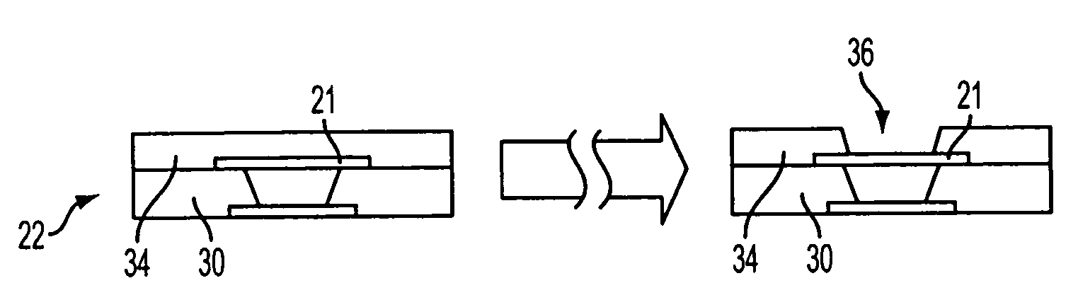
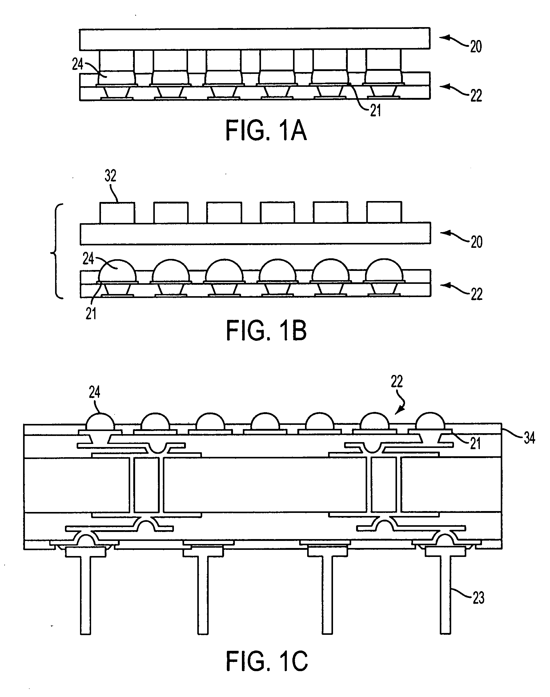
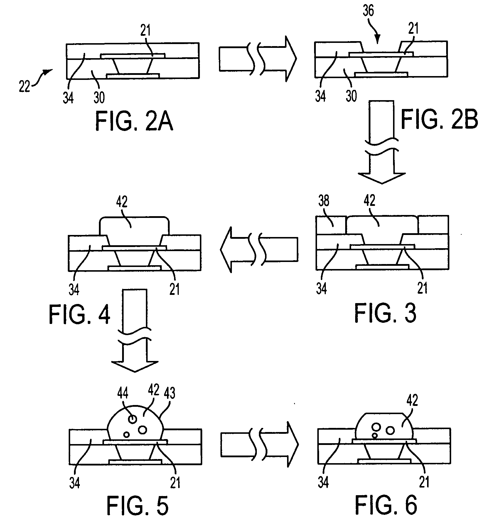
[0019] In an exemplary embodiment of the invention, a method of forming solder bumps is provided. A layer of metal may be formed over a bump pad on a package substrate. The layer of metal may include various discrete layers of metal, which may or may not be formed from the same material. A layer of solder may then be formed over the layer of metal. The solder layer may be formed directly on top of the metal layer. The solder layer may be formed by a solder printing process. The layer of metal may be thicker than the solder layer. The solder layer may then undergo reflow processing. The layer of metal may reduce the amount of solder used in forming a solder bump. By forming a solder bump as a combi...


PUM


Abstract

A layer of metal may be formed under a layer of solder in forming solder bumps. The metal may reduce the amount of solder necessary and may result in a corresponding reduction in solder defects.

Description

BACKGROUND OF THE INVENTION [0001] When using known solder bump formation techniques, voids may form in the solder bumps during formation and reflow. The number of voids in the solder bumps may vary greatly among the different solder bumps on the package substrate. The presence of the voids can have a detrimental effect on the performance of the integrated circuit device. The voids may cause a failure at a maximum current through the semiconductor device. Additionally, current processes used to form solder bumps may result in the failure to form a solder bump at a point where a solder bump should have been be formed and an open failure due to low volume solder bumps, or a short failure due to large volume solder bumps. [0002] There have been great advances in the optimization of solder print printing conditions and solder reflow profiles for reducing solder bump voids, missing bumps and low and large volume solder bumps. However, there are no robust processes currently available to ...

Claims


Application Information

Patent Timeline
IPC IPC(8): H01L21/44
CPCH01L23/49816H01L24/11H01L24/12H01L2224/13099H01L2924/01029H01L2924/01078H01L2924/14H01L2924/15312H05K3/243H05K3/28H05K3/3473H05K3/4007H05K2201/0367H05K2201/09481H05K2203/054H05K2203/0577H01L2924/01006H01L2924/01033H01L2924/014H01L2224/05573H01L2224/05568H01L2924/00014H01L2224/0554H01L2224/05599H01L2224/0555H01L2224/0556
Inventor HORI, YUJI
Owner INTEL CORP
Why Eureka
Try Eureka