Electron multiplier unit and photomultiplier including the same

a technology of electron multiplier and photomultiplier, which is applied in the directions of electron multiplier details, multiplier electrode arrangement, electric discharge tube, etc., can solve the problems of weight of detector parts and impediment to reduce weight and size of apparatus, and achieve the effect of adequate gain and efficient housing

Active Publication Date: 2006-07-27
HAMAMATSU PHOTONICS KK
View PDF3 Cites 0 Cited by
  • Summary
  • Abstract
  • Description
  • Claims
  • Application Information

AI Technical Summary

Benefits of technology

[0012] For example, a γ-camera device used as a medical inspection system is provided with at least a pair of upper and lower camera heads, and each camera head has a structure in which a plurality of photomultipliers are entirely covered by the Pb shield except for a detection window for exposing face plates of the photomultipliers arrayed in a two-dimensional pattern. The number of photomultipliers used has to increase for improvement in detection resolution, and, naturally, the increase of weight of the detector part including the heavy metal shield will pose an impediment to reduction of weight and size of apparatus.
[0013] Then the aforementioned Documents introduce the structure for decreasing the axial length (cylinder length) of the photomultipliers used, in order to reduce the gross weight of the heavy metal shield without degradation of detection resolution.
[0015] The present invention has been accomplished in order to solve the problem as discussed above, and an object of the invention is to provide an electron multiplier unit in a structure for enabling further reduction of the cylinder length, while achieving a high gain and maintaining or further improving the excellent fast response, and a photomultiplier including it.
[0019] In the electron multiplier unit according to the present invention, a total length TL of the travel path of secondary electrons, i.e., an electron travel distance from the first dynode to the anode can be kept not less than two times, preferably four times, a distance D between the first support member and the second support member (a width of the space where the dynodes and others are located). By setting the cascade multiplication structure for obtaining an adequate gain, in the width D in this manner, it becomes feasible to further decrease the cylinder length of a photomultiplier tube to which the electron multiplier unit is applied.
[0021] In the electron multiplier unit according to the present invention, the inlet aperture provided in the first support member is preferably located so that a center of the inlet aperture deviates from a center of the first support member. In a photomultiplier to which the electron multiplier unit is applied, the center of the inlet aperture is located so as to deviate from a tube axis AX. This is for the purpose of efficiently housing the cascade multiplication structure, without increase in the diameter of the first support member or the tube cylinder.
[0022] Furthermore, the structure for cascade multiplication in the electron multiplier unit can be constructed of only box type dynodes, or of a combination of various types of dynodes. For example, the cascade multiplication structure from the second dynode to the anode, or the cascade multiplication structure from a third dynode to the anode may be replaced by grid type or mesh type dynodes. Normally, in the case of the mesh type dynodes, electrons pass through the mesh (η=40%), and it is thus necessary to use ten or more stages of dynodes in order to achieve an adequate gain. In contrast, the electron multiplier unit of the present invention involves preliminary multiplication of the secondary electrons emitted from the first dynode, by means of the second dynode or by means of the second and third dynodes, and thus it can achieve an adequate gain even by a dynode unit having a smaller number of stages.

Problems solved by technology

The number of photomultipliers used has to increase for improvement in detection resolution, and, naturally, the increase of weight of the detector part including the heavy metal shield will pose an impediment to reduction of weight and size of apparatus.

Method used


Image

  • Electron multiplier unit and photomultiplier including the same
  • Electron multiplier unit and photomultiplier including the same
  • Electron multiplier unit and photomultiplier including the same

Examples


first embodiment

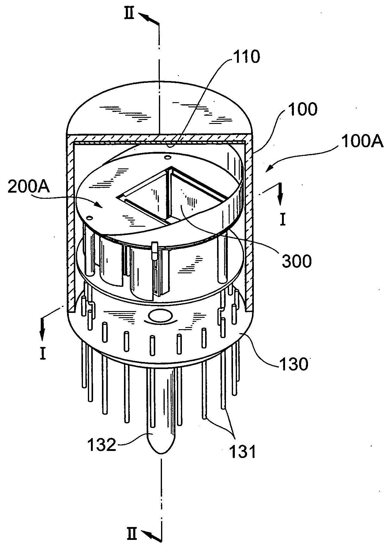
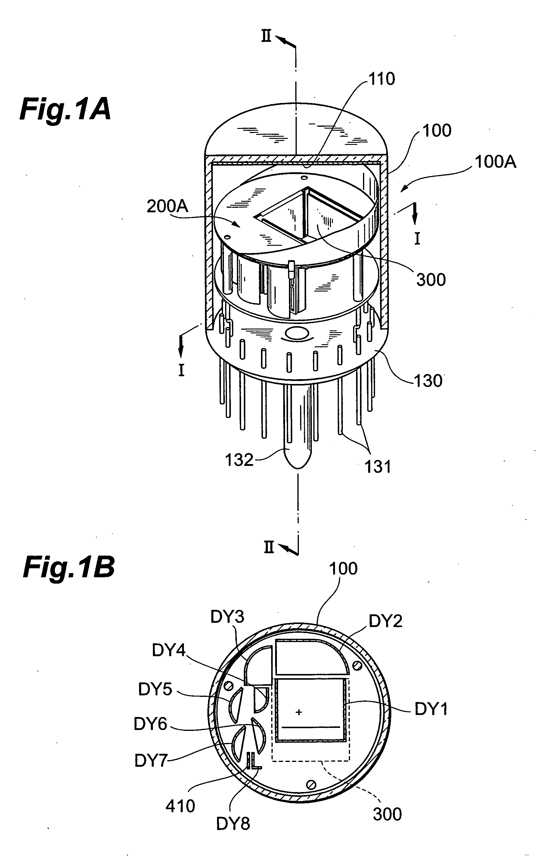
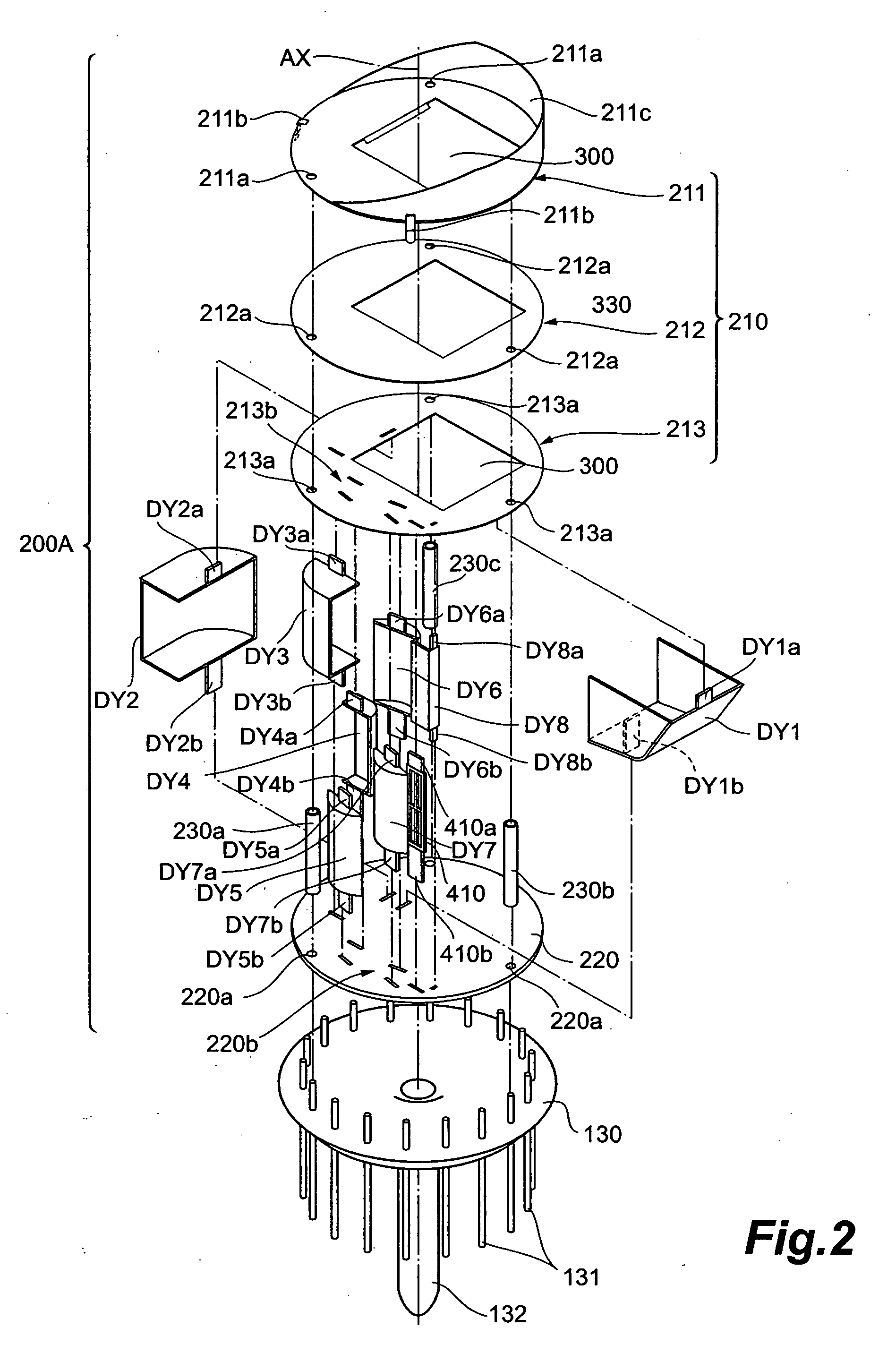
[0047]FIG. 2 is an assembling process chart for explaining the structure of the electron multiplier unit 200A shown in FIG. 1A (the electron multiplier unit according to the present invention).

[0048] As shown in FIG. 2, the electron multiplier unit 200A is comprised of a first support member 210 provided with an inlet aperture 300 for letting the photoelectrons from the cathode 110 pass; a second support member220 arranged in parallel with the first support member 210 along the tube axis AX; first to seventh dynodes DY1-DY7, an anode 410, and a reflection type dynode DY8 placed in the space between these first and second support members 210, 220 and each held by the first and second support members 210, 220. The distance between the first and second support members 210, 220 is defined by hollow ceramic pipes 230a to 230c. The first dynode DY1 is provided with an upper fixing piece DY1a and a lower fixing piece DY1b so as to be held by the first and second support members 210, 220. S...

second embodiment

[0078]FIG. 12A is a perspective view showing a structure of a grid type dynode unit 500 applicable as a part of the electron multiplier unit according to the present invention (the electron multiplier unit according to the present invention). FIG. 12B is a sectional view of the grid type dynode unit 500 along line IV-IV in FIG. 12A. The dynode unit 500 shown in FIGS. 12A and 12B has a multi-stage configuration of grid type dynodes, but may have a multi-stage configuration of mesh type dynodes.

[0079] As shown in FIGS. 12A and 12B, the grid type dynode unit 500 is composed of a focusing electrode plate 430, dynode plates 510 set at predetermined intervals by ceramic spacers 520 each made of an insulating material, and an anode plate 410.

[0080] Each of the focusing electrode plate 430 and the anode plate 410 is provided with an upper fixing piece 500a. Each of the focusing electrode plate 430, dynode plates 510, and anode plate is provided with a lower fixing piece 500b to be electric...


PUM


Abstract

This invention relates to an electron multiplier unit and others enabling cascade multiplication of electrons through successive emission of secondary electrons in multiple stages in response to incidence of primary electrons. The electron multiplier unit has a first support member provided with an inlet aperture for letting primary electrons in, and a second support member located so as to face the first support member. The first support member is provided with a focusing electrode functioning to alter trajectories of the primary electrons, in order to guide the primary electrons to the inlet aperture. These first and second support members hold an electron multiplication section for the cascade multiplication and an anode. The electron multiplication section comprises at least a first dynode of a box type and a second dynode having a reflection type secondary electron emission surface located so as to face the first dynode and arranged to receive secondary electrons from the first dynode and to emit secondary electrons to a side where the first dynode is located. The anode is located at a position where the secondary electrons emitted from the first dynode do not directly arrive, and the second dynode alters a travel path of secondary electrons so as to be kept in a space between the first and second support members.

Description

RELATED APPLICATIONS [0001] This is a Continuation-In-Part application of the Patent application Ser. No. 11 / 080,665 filed on Mar. 16, 2005 by the same Applicant, now pending.BACKGROUND OF THE INVENTION [0002] 1. Field of the Invention [0003] The present invention relates to an electron multiplier unit enabling cascade multiplication of electrons through successive emission of secondary electrons in multiple steps in response to incidence of primary electrons, and to a photomultiplier including the same. [0004] 2. Related Background Art [0005] The following conventional technologies are known as techniques prior to the electron multiplier unit and the photomultiplier including it according to the present invention. [0006] Japanese Patent Application Laid-Open No. 7-245078 [0007] Japanese Patent Application Laid-Open No. 4-315758 [0008] WO98 / 33202 [0009] U.S. Pat. No. 5,914,561 SUMMARY OF THE INVENTION [0010] The Inventor studied the above-cited conventional technologies and found th...

Claims


Application Information

Patent Timeline
Patent Type & Authority Applications(United States)
IPC IPC(8): H01J43/18
CPCH01J43/18H01J43/22H01J43/26
Inventor NAKAMURA, KIMITSUGUOOHASHI, YOUSUKEOHISHI, KEIICHIITO, MASUO
Owner HAMAMATSU PHOTONICS KK
Why Eureka
Try Eureka