Resonant gate drive circuits

a gate drive and circuit technology, applied in the direction of electronic switching, efficient power electronics conversion, pulse technique, etc., can solve the problems of gate drive loss, gate drive loss increase, and penalty on overall converter efficiency. significant, so as to reduce gate drive loss and other losses.

Inactive Publication Date: 2006-08-03
GANPOWER SEMICON FOSHAN LTD
View PDF14 Cites 57 Cited by
  • Summary
  • Abstract
  • Description
  • Claims
  • Application Information

AI Technical Summary

Benefits of technology

The technical effect of this patent is to create a circuit that reduces the energy lost when driving the gates of switches with high input capacity.

Problems solved by technology

The technical problem addressed in this patent is how to improve the performance of switching power converters by reducing the impact of the gate driver on conversion efficiency, particularly in cases such as high frequency, low power applications. Existing solutions like traditional gate drives and resonant gate drivers have limitations including lost efficiencies, complex designs, difficulty in generating control signals, etc. The patent proposes a new solution to overcome these difficulties and achieve better results.

Method used


Image

  • Resonant gate drive circuits
  • Resonant gate drive circuits
  • Resonant gate drive circuits

Examples


embodiment 1 (

Reduced Pulse Embodiment 1 (2-Pulse)

[0170] If pulse 2 is eliminated from S2 and pulse 5 is eliminated from S4 in FIG. 22(a), energy can be saved for these switches in the form of gate loss and output loss (CV2) at turn-on. The body diodes (or external diodes) can be used to clamp the voltage across the inductor, allowing negligible current to circulate in the driver. In this case during the clamping interval t3-t4, switch S1 is on along with the body diode of S2. During the other clamping interval t7-t0, switch S3 is on along with the body diode of S4. Waveforms of this embodiment are shown in FIG. 22(b).

embodiment 2 (

Reduced Pulse Embodiment 2 (2-Pulse)

[0171] If pulse 3 is eliminated from S2 and pulse 6 is eliminated from S4 in FIG. 22(a), energy can be saved for these switches in the form of gate loss. The body diodes (or external diodes) can be used to provide the current paths when the energy is returned to the line. In this case during the energy return interval t2-t3, switch S1 is on along with the body diode of S4. During the other energy return interval t6-t7, switch S3 is on along with the body diode of S2. Waveforms of this embodiment are shown in FIG. 22(c)

embodiment 3 (

Reduced Pulse Embodiment 3 (1-Pulse)

[0172] The above two alternative embodiments may be combined by eliminating pulses 2 and 3 from S2, and pulses 5 and 6 from S4, in FIG. 22(a). Waveforms of this embodiment are shown in FIG. 22(d).

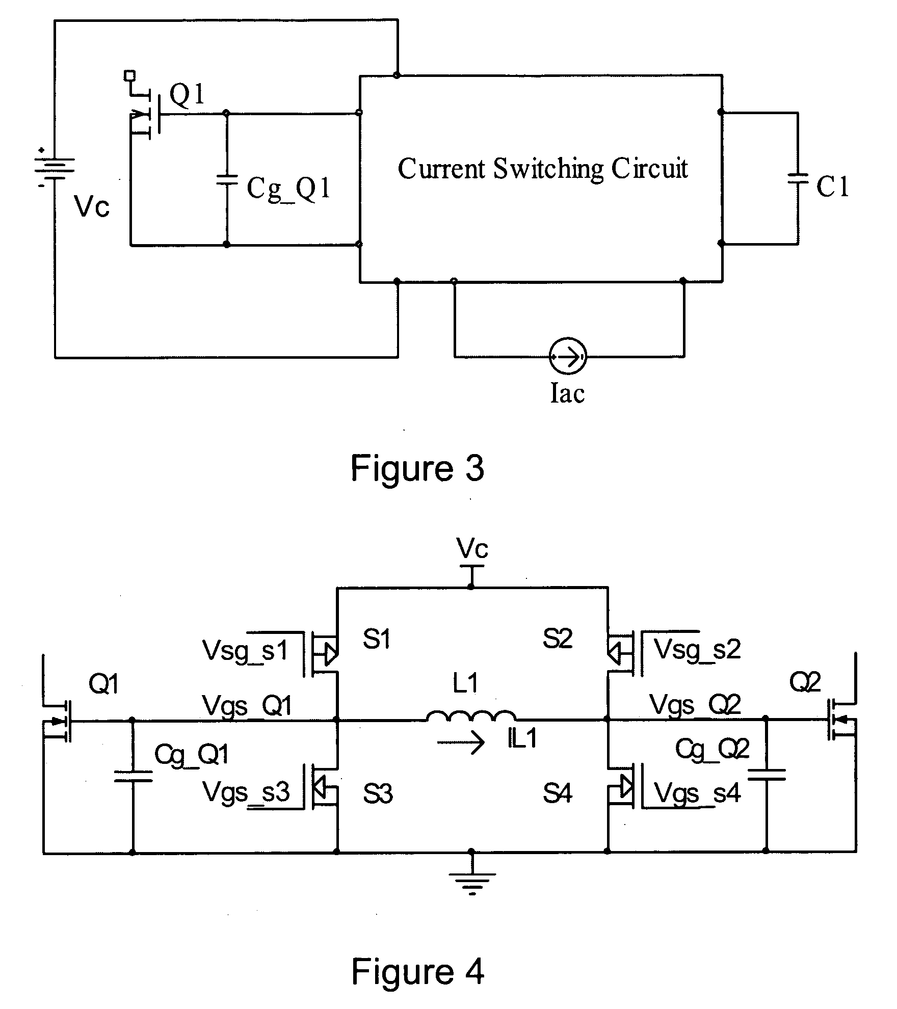
4.4 High-Side Drive Implementation

[0173] This resonant gate driver may be adapted for high-side drive of non-ground referenced MOSFET switches using a bootstrap circuit consisting of a diode, Db, and capacitor, Cb, as illustrated in FIG. 23. The equivalent gate capacitance of the power switch Q is not shown.

4.5 Dual High-Side and Low-Side Drive Implementation

[0174] The high-side driver shown in FIG. 23 may be utilized along with the low-side driver of FIG. 21 to drive both switches in a bridge-leg configuration, such as, for example, a synchronous buck converter, a full-bridge converter, a half-bridge converter, an active clamp forward converter, or a resonant converter with a full-bridge or half-bridge inverter. An example of such a circuit for dri...


PUM


Abstract

A resonate gate drive circuit for driving at least one power switching device recovers energy loss for charging and discharging the gate capacitance of the power switching devices. The gate drive circuit uses a current source to charge and discharge the gate capacitance with a high current, reducing the switching loss of the power switching device. The gate drive circuit comprises four semiconductor bidirectional conducting switching devices connected in a full-bridge configuration. An inductor connected across the bridge configuration provides the current source. The gate drive circuit may be used in single and dual high-side and low-side, symmetrical or complementary, power converter gate drive applications.

Description


Claims


Application Information

Patent Timeline
Owner GANPOWER SEMICON FOSHAN LTD
Why Eureka
Try Eureka