

Method of forming buried isolation regions in semiconductor substrates and semiconductor devices with buried isolation regions
a technology of semiconductor substrate and isolation region, which is applied in the direction of semiconductor devices, electrical equipment, nanotechnology, etc., can solve the problems of inhibiting the optimal operation of devices formed in the silicon layer by the buried oxide layer
- Summary
- Abstract
- Description
- Claims
- Application Information
AI Technical Summary
Problems solved by technology
Method used
Image

Examples
first embodiment
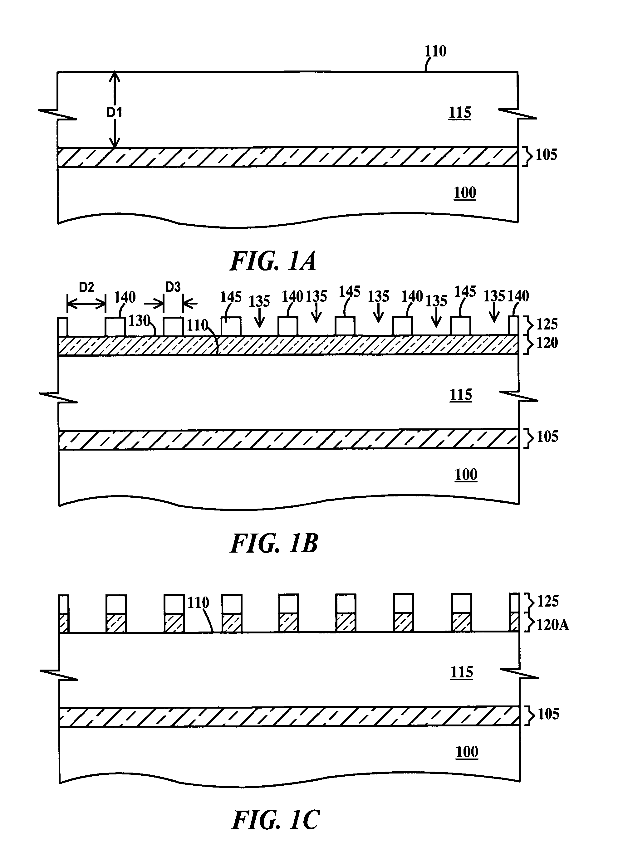
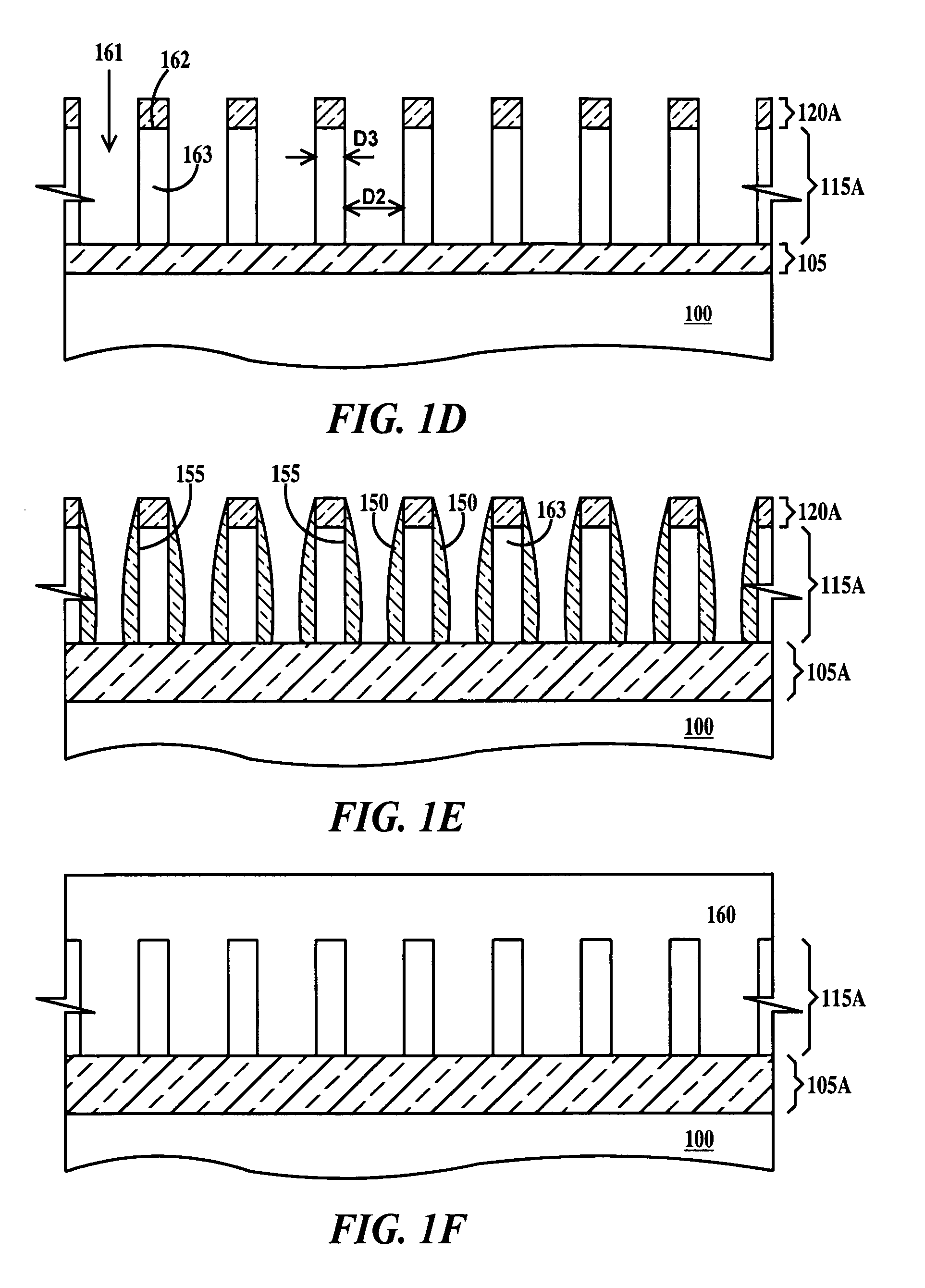
[0017]FIGS. 1A through 1H are partial cross-sectional views illustrating the steps to form a buried isolation region in a semiconductor substrate according to the present invention. In FIG. 1A, a silicon substrate 100 has been exposed to a high power oxygen implantation to create an oxygen rich layer 105 a distance D1 from a top surface 110 of substrate 100 into the substrate. Oxygen rich layer 105 defines an upper portion of silicon substrate 100 as a silicon layer 115 between the oxygen rich layer and the top surface of the substrate. Oxygen rich layer 105 may contain regions of silicon dioxide. As the exact stoichiometry of oxides of silicon can vary somewhat in semiconductor structures, for the purposes of the present invention, the term silicon dioxide includes compounds of silicon and oxygen having the specific formulas SiO2 as well as the general formula SixOy. In one example, distance D1 is about 20 nm to about 100 nm.
[0018] In FIG. 1B, a hard mask layer 120 is formed on top...
second embodiment
[0035]FIGS. 2A through 2E are partial cross-sectional views illustrating the steps to form a buried isolation region in a semiconductor substrate according to the present invention. In FIG. 2A, a silicon dioxide layer 215 is formed on a top surface 220 of a silicon substrate 225. In one example silicon dioxide layer 215 is about 5 nm to about 100 nm thick.
[0036] In FIG. 2B, nano-mask layer 125 is formed on top surface 230 of silicon dioxide layer 215. Nano-mask layer 125 has been described supra in relationship to the first embodiment of the present invention.
[0037] In FIG. 2C, silicon dioxide layer 215 (see FIG. 2B) is removed (for example by a RIE process) to form a patterned silicon dioxide layer 215A and exposing silicon substrate 225 wherever the silicon dioxide layer 215 is not protected by nano-mask layer 125. Patterned silicon dioxide layer 215A comprises void regions 231 extending from a top surface 232 of patterned silicon layer 215A to top surface 220 of substrate 225 an...
third embodiment
[0040]FIGS. 3A through 3E are partial cross-sectional views illustrating the steps to form a buried isolation region in a semiconductor device in a semiconductor substrate according to the present invention. In FIG. 3A, silicon dioxide layer 215 is formed on a top surface 220 of a silicon substrate 225. In one example, silicon dioxide layer 215 is about 5 nm to about 100 nm thick. A silicon nitride layer 245 is formed on top surface 230 of silicon dioxide layer 215. In one example, silicon nitride layer 245 is about 50 nm to about 100 nm thick. An opening 250 is formed in silicon nitride layer 245 exposing silicon dioxide layer 215 in the opening.
[0041] In FIG. 3B, nano-mask 125 is formed on a top surface 230 of silicon dioxide layer 215. Nano-mask layer 125 has been described supra in relationship to the first embodiment of the present invention.
[0042] In FIG. 3C, silicon dioxide layer 215 (see FIG. 3B) is removed (for example by a RIE process selective to silicon nitride) to form...
PUM
 Abstract
Description
Claims
Application Information