Nanostructured device

a nanostructured, device technology, applied in the direction of nanotechnology, semiconductor devices, electrical devices, etc., can solve the problems of difficult application of standard processes for nanowire removal, selective nanowire growth yielding non-uniform growth conditions, etc., to avoid complex nanowire removal steps, improve process integration, and reduce process time

Active Publication Date: 2011-10-06
NANOSYS INC
View PDF4 Cites 59 Cited by
  • Summary
  • Abstract
  • Description
  • Claims
  • Application Information

AI Technical Summary

Benefits of technology

[0008]One object of the invention is to overcome problems related to contacting nanowire structures, and in particular nanowire LED's, namely to improve process integration and decrease process time since the invention enables contacting of the terminals directly. In particular, the invention enables use of the same processing steps and homogeneous growth conditions for the entire substrate, minimizing for example edge effects and avoiding complicated nanowire removal steps. Further, the invention is applicable on all nanostructured devices with vertical nanowires that are electrically contacted from a buffer layer or a substrate.

Problems solved by technology

However, standard processes are difficult to apply for nanowire removal, since typical etch processes do not work well for this kind of structure and selective nanowire growth yields non-uniform growth conditions.

Method used


Image

  • Nanostructured device
  • Nanostructured device
  • Nanostructured device

Examples


Embodiment Construction

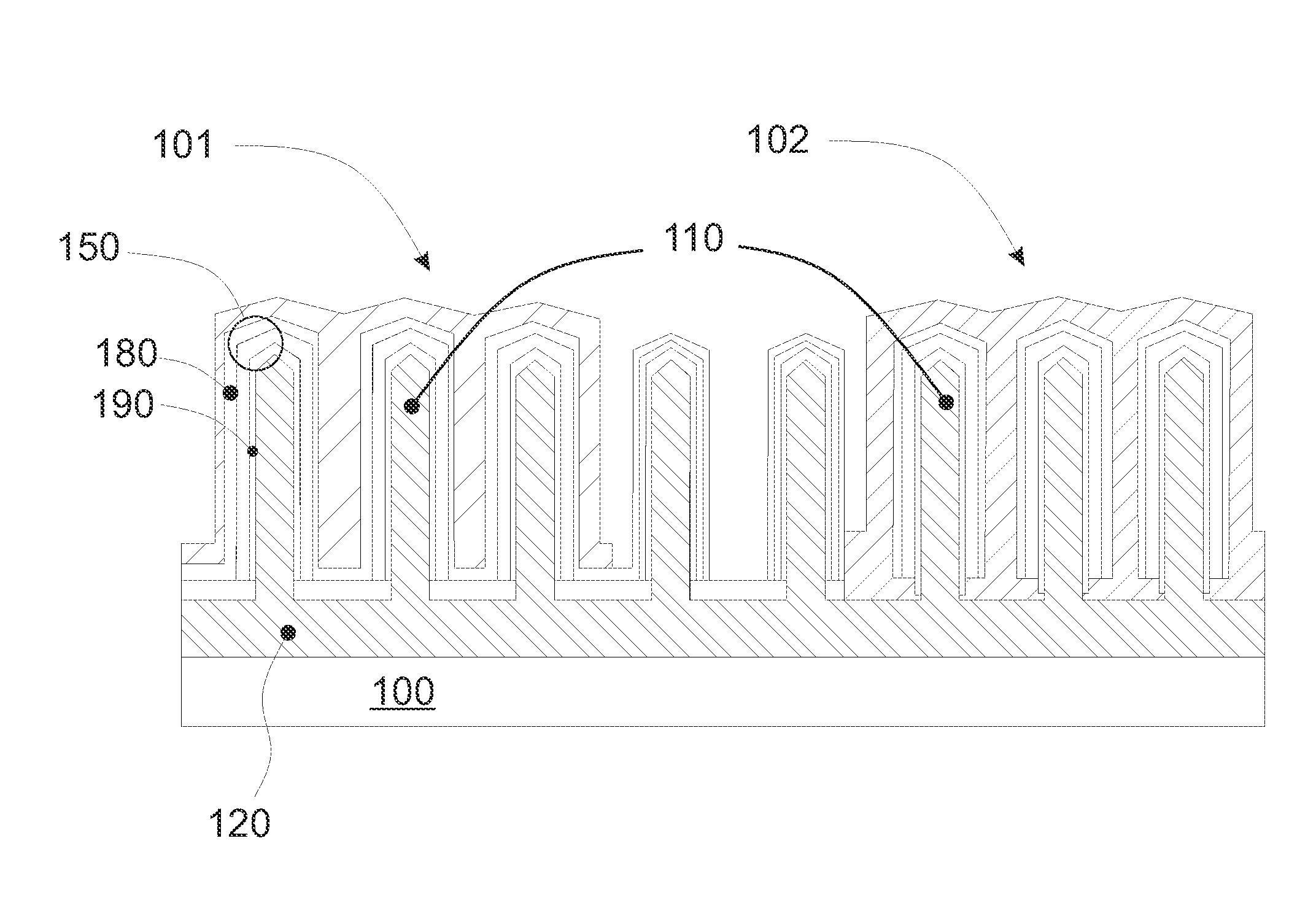
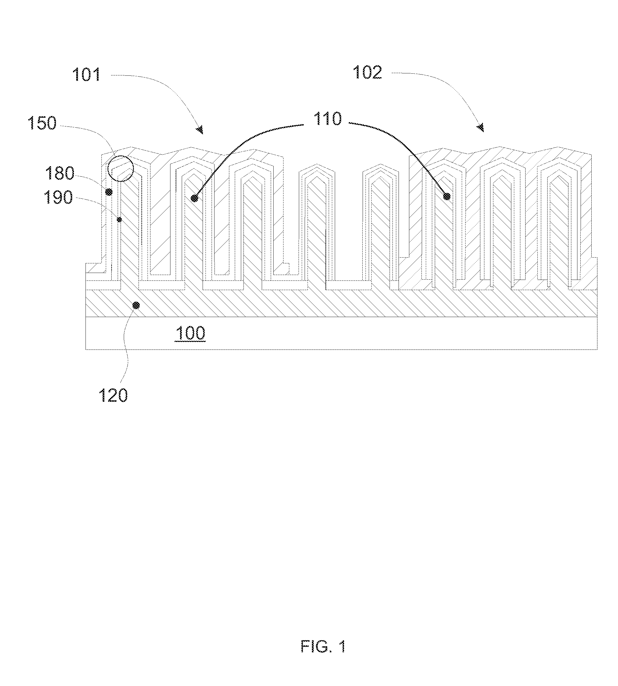
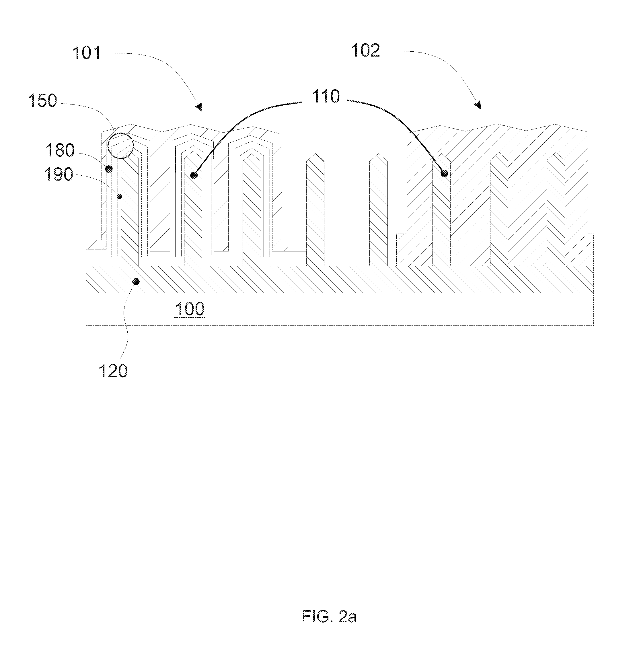
[0015]In the following, the contacting of nanostructured devices is mainly described in terms of a nanostructured LED device, however not limited to this. Prior art nanostructured devices of this kind are known from for example U.S. Pat. No. 7,396,696 and WO2008048704.

[0016]In the field of art nanowires are usually interpreted as one dimensional nanostructures that is in nanometer dimensions in its diameter. As the term nanowire implies it is the lateral size that is on the nano-scale whereas the longitudinal size is unconstrained. Such one dimensional nanostructures are commonly also referred to as nanowhiskers, one-dimensional nano-elements, nanorods, nanotubes, etc. Generally, nanowires are considered to have at least two dimensions each of which are not greater than 300 nm. However, the nanowires can have a diameter or width of up to about 1 μm. The one dimensional nature of the nanowires provides unique physical, optical and electronic properties. These properties can for examp...


PUM

PropertyMeasurementUnit
widthaaaaaaaaaa
conductionaaaaaaaaaa
charge carrieraaaaaaaaaa

Abstract

A nanostructured device according to the invention comprises a first group of nanowires protruding from a substrate where each nanowire of the first group of nanowires comprises at least one pn- or p-i-n-junction. A first contact, at least partially encloses and is electrically connected to a first side of the pn- or p-i-n-junction of each nanowire in the first group of nanowires. A second contacting means comprises a second group of nanowires that protrudes from the substrate, and is arranged to provide an electrical connection to a second side of the pn- or p-i-n-junction.

Description

TECHNICAL FIELD OF THE INVENTION[0001]The present invention relates to nanostructured device comprising nanowires. In particular the invention relates to contacting of nanostructured LEDs.BACKGROUND OF THE INVENTION[0002]Nanowire based semiconductor devices such as LEDs (Light Emitting Diodes), FETs (Field Effect Transistors), diodes, solar cells and detectors are comprised of semiconductor nanowires or arrays of semiconductor nanowires grown on the surface of a substrate, for example silicon, sapphire, GaAs, GaP, GaN. Often, a planar buffer layer is grown first on the substrates and subsequently the semiconductor nanowires or the arrays of semiconductor nanowires are grown on the surface of the buffer layer. The buffer layer is used as the base layer for growing the nanowires. Additionally, it can serve for as an electrical current transport layer.[0003]The basic process of nanowire formation on substrates is by particle assisted growth or the so-called VLS (vapour-liquid-solid) me...

Claims


Application Information

Patent Timeline
Patent Type & Authority Applications(United States)
IPC IPC(8): H01L33/04H01L21/20B82Y99/00
CPCB82Y10/00H01L29/0665H01L29/0673H01L29/0676H01L29/417H01L31/035281H01L33/06H01L33/38Y02E10/50H01L29/413B82Y40/00H01L21/02603H01L29/0669H01L33/24H01L33/00H01L33/12H01L21/0425H01L29/068
Inventor KONSEK, STEVEN LOUISMARTYNOV, YOURIIOHISSON, JONASHANBERG, PETER JESPER
Owner NANOSYS INC
Why Eureka
Try Eureka