Semiconductor device and process for producing the same

a semiconductor device and process technology, applied in the direction of printed circuit, sustainable manufacturing/processing, final product manufacturing, etc., can solve the problems of affecting the electrical characteristics of the semiconductor device, and affecting the bondability of the bumps

Inactive Publication Date: 2006-08-10
SONY CORP
View PDF7 Cites 21 Cited by
  • Summary
  • Abstract
  • Description
  • Claims
  • Application Information

AI Technical Summary

Problems solved by technology

However, for example, when the bumps 2 and 4 are ball-shaped, a slight misalignment greatly affects bondability of the bumps and the electrical characteristics of the semiconductor device.
In some cases, open failure or shortcircuit failure may occur.
However, in the production method described in the above Patent Document 1, when a metal bump of the semiconductor chip is pu

Method used


Image

  • Semiconductor device and process for producing the same
  • Semiconductor device and process for producing the same
  • Semiconductor device and process for producing the same

Examples


Embodiment Construction

[0019] An embodiment of the present invention will be described in detail below with reference to the drawings.

[0020] In a semiconductor-device production method according to the present invention, flip chip bonding for electrically connecting electrodes of a semiconductor chip and a mount substrate by bonding bumps is adopted to mount the semiconductor chip on the mount substrate. A specific procedure of the method will be described below.

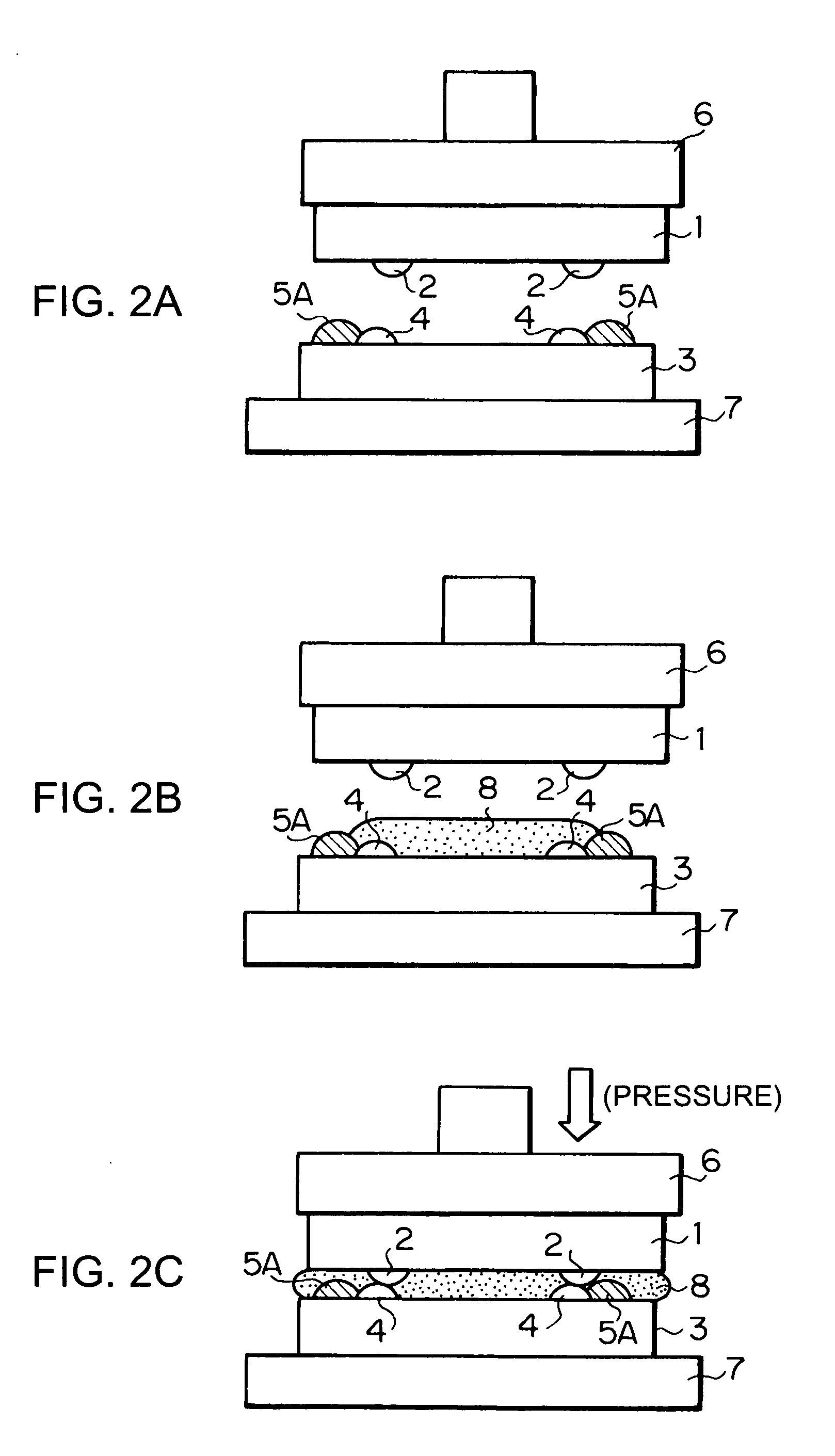
[0021] FIGS. 1 to 3B are explanatory views showing a specific example of a semiconductor-device production method according to an embodiment of the present invention. In the description of this embodiment, components similar to those of the above-described conventional art are denoted by the same reference numerals.

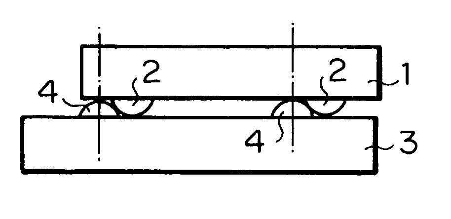
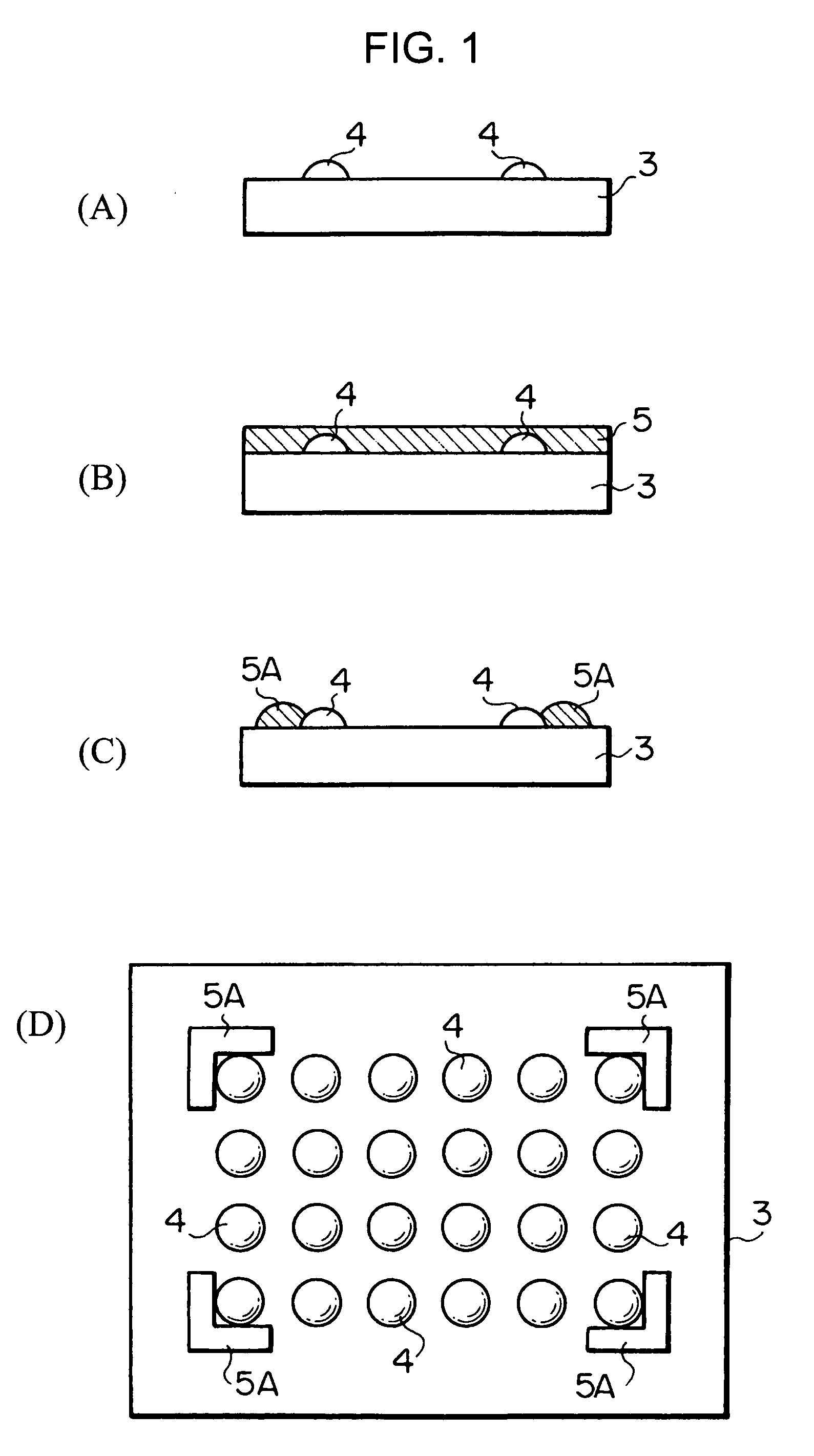
[0022] First, as shown in FIG. 1(A), a plurality of bumps 4 are formed on a chip mount surface of a mount substrate 3 on which a semiconductor chip is to be mounted. Each of the bumps 4 is a metal bump made of a metal that is not mel...


PUM


Abstract

When a semiconductor chip is mounted on a mount substrate by bonding bumps, bonding failure is caused by misalignment between the bumps.
Before a semiconductor chip having a plurality of bumps is mounted on a mount substrate (3) having a plurality of bumps (4) by flip chip bonding, a resist layer (5) having a thickness larger than that of the bumps (4) is formed on the mount substrate (3) with the bumps. By patterning the resist layer (5), projecting guides (5A) of semicircular cross section are formed on the mount substrate (3) so as to protrude near the bumps (4) and from a surface on which the bumps (4) are provided, and to have guide faces (curved faces) pointing toward the bumps (4).

Description

TECHNICAL FIELD [0001] The present invention relates to a semiconductor-device production method suitably used to mount a semiconductor chip on a mount substrate by bonding bumps, and to a semiconductor device produced by the production method. BACKGROUND ART [0002] At present, SIPs (System in Package), which are obtained by combining a plurality of LSI (Large Scale Integration) devices, such as a CPU (central processing unit) and a memory, into one package, are known as a type of package for a high-performance semiconductor device. Some SIPs adopt a package form in which a plurality of semiconductor chips are mounted on a common mount substrate (interposer). Some other SIPs adopt, as a mount substrate, a semiconductor chip having a diameter larger than that of a semiconductor chip to be mounted thereon (chip-on-chip SIPs). [0003] As a method for mounting a semiconductor device by using such an SIP package form, flip chip bonding has recently been practically available in order to i...

Claims


Application Information

Patent Timeline
IPC IPC(8): H01L21/48H01L21/50H01L21/56H01L21/60H01L23/498H05K3/30
CPCH01L21/563H01L23/49811H01L24/32H01L24/81H01L2224/16145H01L2224/16225H01L2224/27013H01L2224/81801H01L2224/83051H01L2224/83192H01L2924/01004H01L2924/01005H01L2924/01013H01L2924/01015H01L2924/01018H01L2924/01027H01L2924/01033H01L2924/01039H01L2924/0105H01L2924/01078H01L2924/01079H01L2924/01082H01L2924/12044H05K3/303H05K2201/09909H05K2201/10674H05K2203/167H01L2924/01006H01L2924/01019H01L2924/01068H01L2924/014H01L24/29H01L2224/73204H01L2224/73103H01L2224/10165H01L2224/81136H01L2224/8114H01L2224/73104H01L2224/16105H01L2224/81193H01L2224/81194Y02P70/50
Inventor SENDA, AYUMI
Owner SONY CORP
Why Eureka
Try Eureka