This helps you quickly interpret patents by identifying the three key elements:
Problems solved by technology
Method used
Benefits of technology
Benefits of technology
[0013] By thus feeding the Group III element and nitrogen after the feeding of the surface control element, the formation of a nitride layer of Si or the like on the SiC surface can be prevented regardless of the order of feeding of the Group III element and nitrogen. As a result, a good interface can be formed and the need to control the order of feeding of the Group III element and nitrogen can be eliminated.
[0014] In yet another aspect of the invention, the invention provides a crystal growing method comprising the steps of:
Problems solved by technology
While it is expected that the inconsistency in stacked structures can be resolved by the aforementioned method, there are two additional problems in the crystal growth of Group III nitride on SiC surfaces.
One is that the SiC surface is chemically and thermally stable, and it is difficult to control the SiC surface condition unless a high-temperature environment, such as one exceeding 1200° C., is used.
Such high-temperature environment, however, is diffi
Method used
Image
Click on the blue label to locate the original text in one second.
Reading with bidirectional positioning of images and text.
Examples
first embodiment
[0046] Thus, in accordance with the invention, after a SiC surface and a surface with common multiples of the total number of the molecules in the SiC surface and the AlN layer that is deposited thereon are prepared, the AlN layer is grown, whereby AlN can be formed on the SiC surface by layer-by-layer growth or step-flow growth (two-dimensional growth). As a result, defects are less likely to be introduced as compared with the conventional case of three-dimensional island growth, such that high-quality crystal growth can be achieved. During the AlN crystal growth, N may be intermittently fed while an Al beam is shone.
[0047] There are many steps on the SiC surface prior to the AlN growth. The heights of all of the steps preferably correspond to the least common multiples of the total number of the molecules of SiC and AlN. However, it is known that significant effect for achieving higher quality of the AlN crystal can be obtained even if some steps do not have such height as long as...
second embodiment
[0051] Hereafter, a crystal growth method according to the invention is described with reference to the drawings. FIG. 5 shows the steps of the crystal growing method according to the present embodiment. FIG. 6 shows a sequence chart regarding the timing of feeding of growth elements (which is controlled by turning on and off of a shutter, for example, in the case of MBE) before and after the crystal growth of a Group III nitride.
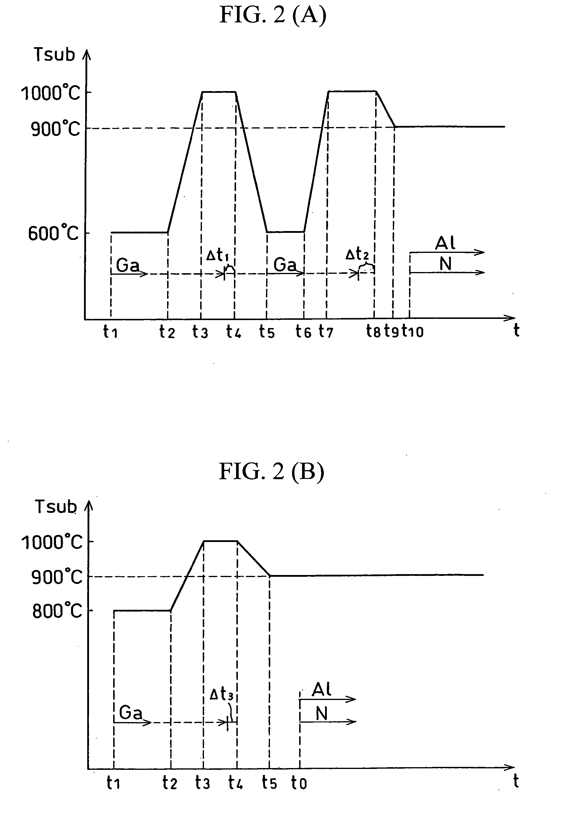
[0052] In the following, the crystal growth step in the present embodiment is described in detail with reference to FIGS. 5 and 6. As shown in FIG. 5(A), initially a washed 4H—SiC(0001)Si substrate 11 is prepared. Then, a clean surface 15 is formed on the surface of the substrate 11, as in the case of the above-described first embodiment. Thereafter, as shown in FIG. 5(B) and FIG. 6, the Al irradiation is carried out first at time t11. At time t12 (t12−t11=10 s, for example), when the surface of the SiC substrate 11 is substantially entirely covered with Al...
third embodiment
[0053] Hereafter, a crystal growing method according to the invention is described with reference to the drawings. FIG. 7 shows the steps of the crystal growing method according to the present embodiment, and FIG. 8 shows a sequence chart regarding the timing of feeding of growth elements (which is controlled by turning on and off of a shutter, for example, in the case of MBE) before and after the crystal growth of a Group III nitride.
[0054] In the following, the crystal growth steps in accordance with the present embodiment will be described with reference to FIGS. 7 and 8. As shown in FIG. 7(A), initially a washed 4H—SiC(0001)Si substrate 21 is prepared. Then a clean surface 25 is formed on the surface of the substrate 21 in the same manner as in the first and second embodiments. Thereafter, as shown in FIG. 7(B) and FIG. 8, at a certain time (time t20), the Ga irradiation is first carried out. Near the growth temperature of AlN, the vapor pressure of Ga is higher than the vapor p...
PUM
Abstract
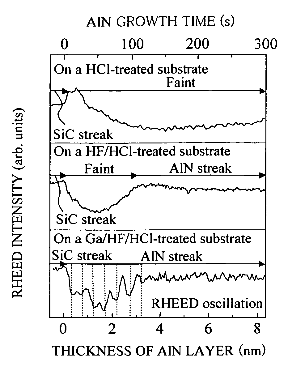
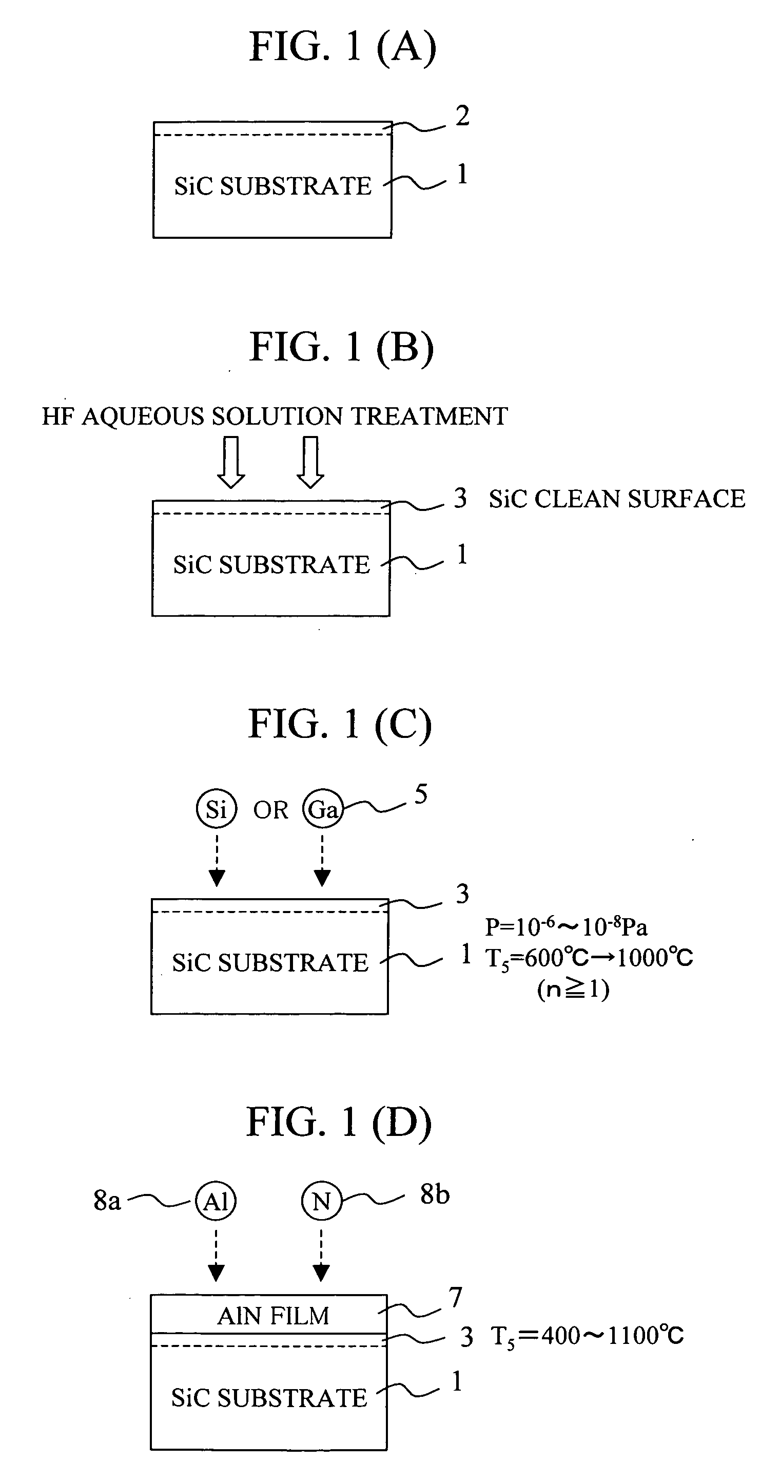
SiC is a very stable substance, and it is difficult to control the condition of a SiC surface to be suitable for crystal growth in conventional Group III nitride crystal growing apparatuses. This problem is solved as follows. The surface of a SiC substrate 1 is rendered into a step-terrace structure by performing a heating process in an atmosphere of HCl gas. The surface of the SiC substrate 1 is then treated sequentially with aqua regia, hydrochloric acid, and hydrofluoric acid. A small amount of silicon oxide film formed on the surface of the SiC substrate 1 is etched so as to form a clean SiC surface 3 on the substrate surface. The SiC substrate 1 is then installed in a high-vacuum apparatus and the pressure inside is maintained at ultrahigh vacuum (such as 10−6 to 10−8 Pa). In the ultrahigh vacuum state, a process of irradiating the surface with a Ga atomic beam 5 at time t1 at temperature of 800° C. or lower and performing a heating treatment at 800° C. or higher is repeated at least once. The temperature is then set to the growth temperature of an AlN film, and the SiC substrate surface 3 is initially irradiated with —Al atoms 8a in ultrahigh vacuum state, followed by the feeding of N atoms 8b.
Description
TECHNICAL FIELD [0001] The present invention relates to a semiconductor crystal growing technology, and more particularly to a technique for growing Group III nitride crystals on an SiC surface. BACKGROUND ART [0002] Hexagonal SiC has a very high heat conductivity, and both electrically conductive and insulating substrates are available. Its lattice constant and coefficient of thermal expansion are relatively close to those of AlN and GaN-based Group III nitrides. Another characteristic of hexagonal SiC is that it is a hexagonal crystal and possesses polarities, as to Group III nitrides. [0003] There are high expectations for the realization of a technology for growing high-quality crystals of Group III nitrides on SiC for applications relating to a buffer layer for the formation of a GaN-based device structure on an SiC substrate, or relating to Group III nitride / SiC heterojunction devices. It has been difficult to grow a high-quality Group III nitride layer on SiC because of the m...
Claims
Application Information
Patent Timeline
Application Date:The date an application was filed.
Publication Date:The date a patent or application was officially published.
First Publication Date:The earliest publication date of a patent with the same application number.
Issue Date:Publication date of the patent grant document.
PCT Entry Date:The Entry date of PCT National Phase.
Estimated Expiry Date:The statutory expiry date of a patent right according to the Patent Law, and it is the longest term of protection that the patent right can achieve without the termination of the patent right due to other reasons(Term extension factor has been taken into account ).
Invalid Date:Actual expiry date is based on effective date or publication date of legal transaction data of invalid patent.

