High power LED housing and fabrication method thereof

a technology of led housing and fabrication method, which is applied in the direction of display means, chemistry apparatus and processes, light and heating apparatus, etc., can solve the problems of burdening manufacture costs and not teaching any fabrication method of package structure, and achieve the effect of stably coupling and efficient heat dissipation

Inactive Publication Date: 2006-08-17
SAMSUNG ELECTRONICS CO LTD
View PDF3 Cites 63 Cited by
  • Summary
  • Abstract
  • Description
  • Claims
  • Application Information

AI Technical Summary

Benefits of technology

[0019] The present invention has been made to solve the foregoing problems of the prior art and it is therefore an object of the present invention to provide an LED housing which can securely fix a neck of a heat conducting part at both sides with a pair of fixing parts, thereby stably coupling the heat conducting part to a housing body made of resin, and allow the fixing parts to spread heat from the heat conducting part to lateral regions of the LED housing, thereby more efficiently spreading heat within the LED housing.
[0020] It is another object of the invention to provide a fabrication method of an LED housing which can fabricate an LED housing easily and stably by carrying out resin molding with a heat conducting part inserted into a pair of fixing parts of a frame to form a housing body, taking a resultant structure out of a mold when resin is cured, and separating the LED housing from the frame. This object is also aimed to use the frame with the fixing parts and an electrical connecting part formed therein as means for fixing the heat conducting part in order to automate fabrication, thereby saving cost and improving productivity.

Problems solved by technology

However, this structure is disadvantageously complicated to obstruct the automation of LED package fabrication as well as require a large number of components to be assembled together, thereby burdening manufacture cost.
Furthermore, this document does not teach any fabrication method of a package structure that can be used in such an insulated structure.

Method used


Image

  • High power LED housing and fabrication method thereof
  • High power LED housing and fabrication method thereof
  • High power LED housing and fabrication method thereof

Examples


Embodiment Construction

[0069] Preferred embodiment of the present invention will now be described in detail with reference to the accompanying drawings.

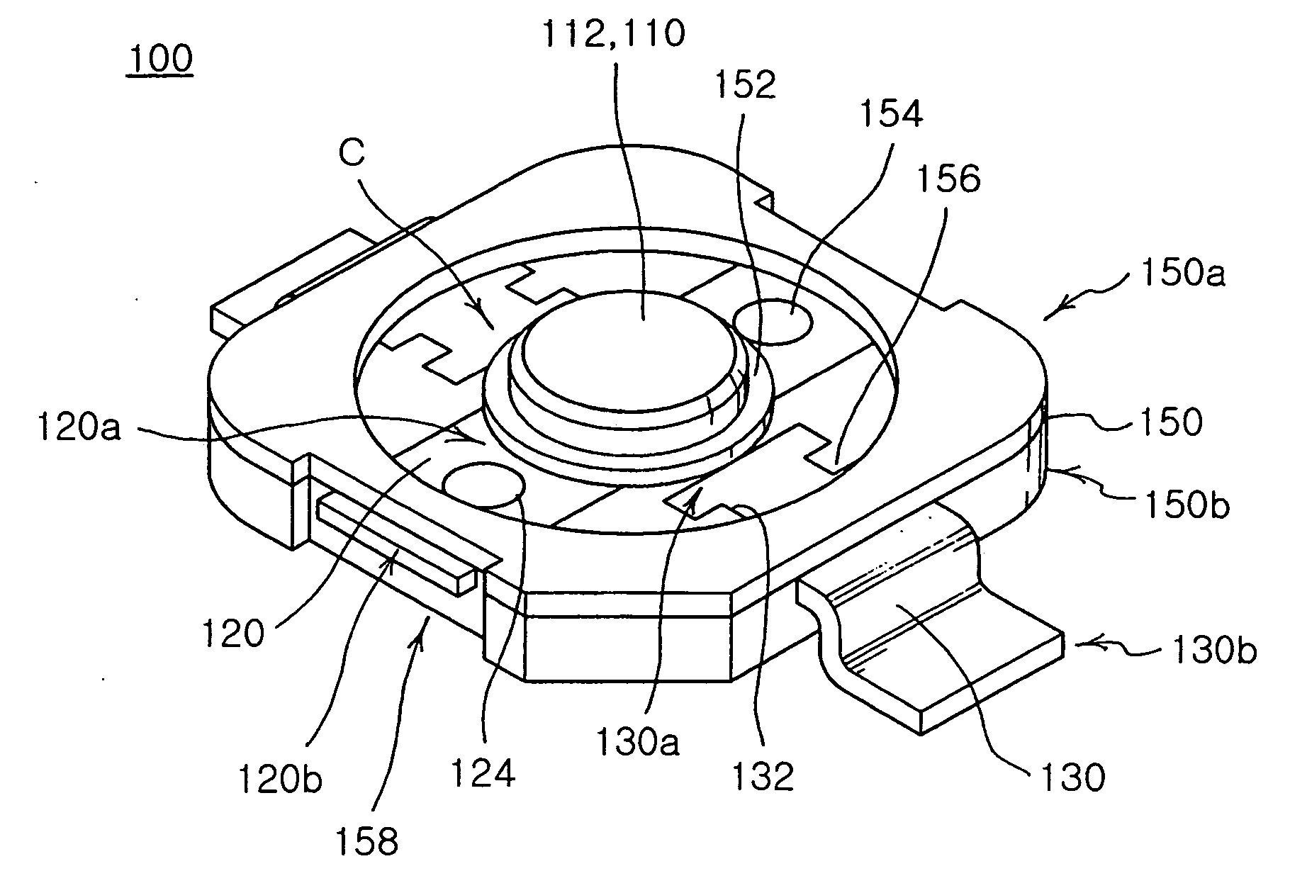
[0070] Referring to FIGS. 3 to 7 first, an LED housing 100 of the invention includes a heat conducting part 110, a pair of fixing parts 120, a pair of electric connecting parts 120 and a housing body 150.

[0071] The heat conducting part 110 is made of a lump of metal preferably having high heat conductivity. The heat conducting part 110 has a chip mounting area 112 on which an LED chip (refer to FIG. 8) is mounted, a heat connecting area 114 opposite to the chip mounting area and a neck 116 of a reduced width between the chip mounting and heat connecting areas 112 and 114.

[0072] The fixing parts 120 each have a holder 122 formed at a first end 120a thereof inside the housing 100, engaged with the neck 116 of the heat conducting part 110. The holders 122 are curved inward with a curvature the same as that of the neck 116 as shown in FIG. 14 to hold the ne...


PUM


Abstract

An LED housing, in which a heat conducting part has a chip mounting area, a heat connecting area opposed to the chip mounting area and a neck between them. Fixing parts have first ends engaged with the neck. An electrical connecting part has a wire connecting area placed adjacent to the chip mounting area and an external power connecting area connected to the wire connecting area. A housing body of molding material integrally holds the heat conducting part, the fixing parts and the electrical connecting part while isolating the electrical connecting part from the heat conducting part. The LED housing fixes the neck of the heat conducting part at both sides, thereby stably coupling the heat conducting part to the housing body. The fixing parts can spread heat from the heat conducting part to lateral regions of the LED housing, thereby more efficiently spreading heat.

Description

CLAIM OF PRIORITY [0001] This application claims the benefit of Korean Patent Application No. 2005-13249 filed on Feb. 17, 2005, in the Korean Intellectual Property Office, the disclosure of which is incorporated herein by reference. BACKGROUND OF THE INVENTION [0002] 1. Field of the Invention [0003] The present invention relates to an LED housing and a fabrication method thereof. More particularly, the LED housing of the present invention can securely fix a neck of a heat conducting part at both sides with a pair of fixing parts, thereby stably coupling the heat conducting part to a housing body made of resin, while allowing the fixing parts to spread heat from the heat conducting part to lateral regions of the LED housing, thereby more efficiently spreading heat within the LED housing. [0004] 2. Description of the Related Art [0005] A Light Emitting Diode (LED) is a semiconductor device that is activated in response to electric current to generate various colors of light. The colo...

Claims


Application Information

Patent Timeline
Patent Type & Authority Applications(United States)
IPC IPC(8): H01L33/00H01L33/56H01L33/64
CPCH01L33/486H01L33/58H01L33/60H01L33/62H01L33/642H01L33/647H01L2224/48091H01L2224/48247H01L2924/00014H01L2924/01019H01L2924/12041Y10S362/80B32B29/002B32B29/06B32B2307/4026B32B2317/122
Inventor KIM, CHANG WOOKLEE, SEON GOO
Owner SAMSUNG ELECTRONICS CO LTD
Why Eureka
Try Eureka