Method to detect NAND-flash parameters by hardware automatically

a hardware and parameter detection technology, applied in the field of parameter detection, can solve the problems of complex interface timing at a nand-flash, inability to boot cpu directly from nand-flash, and difficult read access, and achieve the effect of low cost and small area

Inactive Publication Date: 2006-08-31
AVAGO TECH INT SALES PTE LTD
View PDF4 Cites 174 Cited by
  • Summary
  • Abstract
  • Description
  • Claims
  • Application Information

AI Technical Summary

Benefits of technology

This patent describes a way to make sure computer chips can easily find certain settings on their own when they start up. It also means that these chip can use less expensive flash memory instead of more complicated ones, which saves money and space. Additionally, it allows the chip to run instructions straight out of the flash memory, eliminating the need for extra RAM or NOR-flash memory.

Problems solved by technology

The technical problem addressed in this patent relates to the difficulty of accessing and reading the content of NAND-Flash memory due to its complex interface timings and lack of specific addresses. Conventional methods require a central processing unit (CPU) to control the access cycle, which adds complexity and expense to the system. Additionally, new design variations of NAND-Flash may require changes to the software, firmware, or database to ensure compatibility.

Method used


Image

  • Method to detect NAND-flash parameters by hardware automatically
  • Method to detect NAND-flash parameters by hardware automatically
  • Method to detect NAND-flash parameters by hardware automatically

Examples


Embodiment Construction

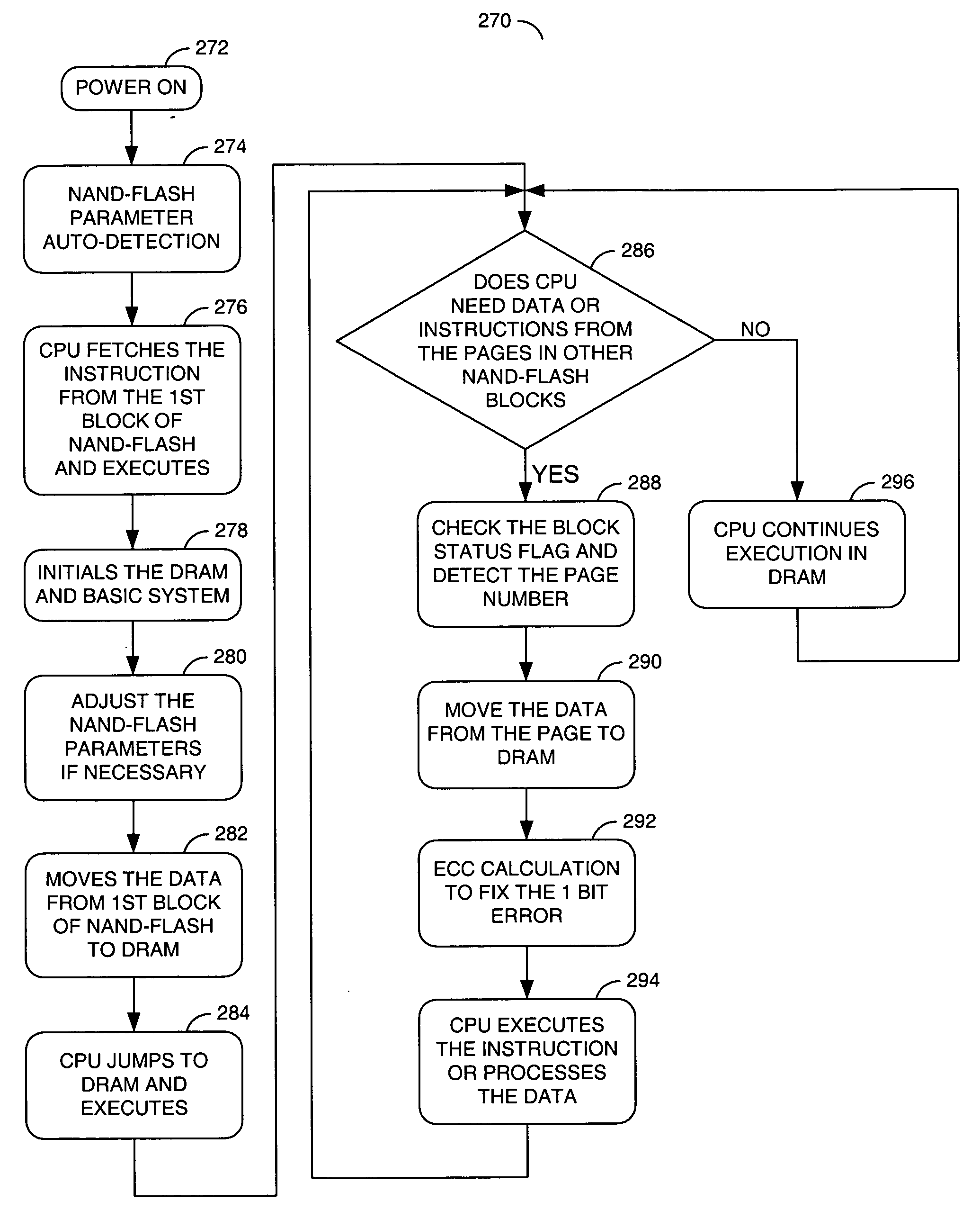
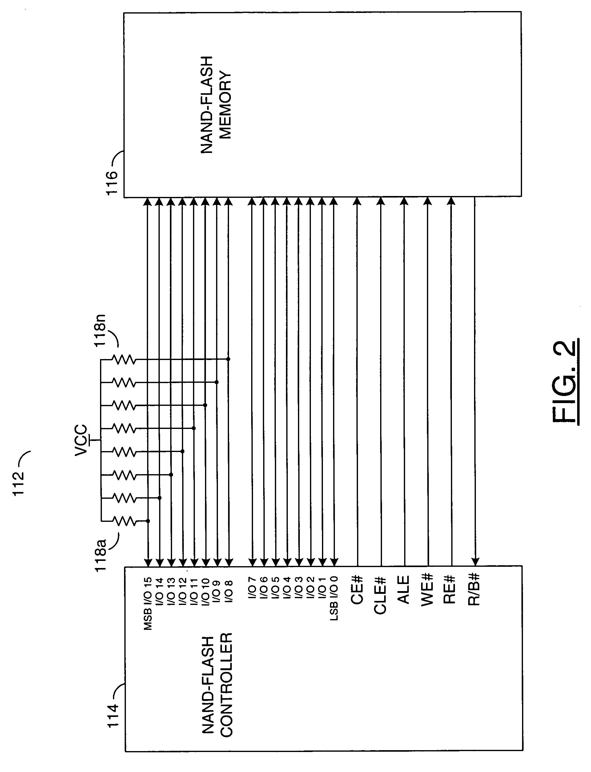
[0016] The present invention provides a method (or process) and a circuit (or system) to automatically detect a plurality of interface parameters of a NAND-Flash memory (or device). Hereafter, “NAND-Flash” generally refers to a NAND-Flash memory and / or a SmartMedia™ card. The invention may be used in application specific integrated circuits (ASIC) that interfaces to one or more NAND-Flash devices. The method / hardware provides automatic detection of the NAND-Flash parameters and thus enables a system or system on a chip (SOC) to be directly boot up from a NAND-Flash memory. In a system without a host central processing unit (CPU), the method / hardware may provide great flexibility in terms of the types of NAND-Flash that may be supported.

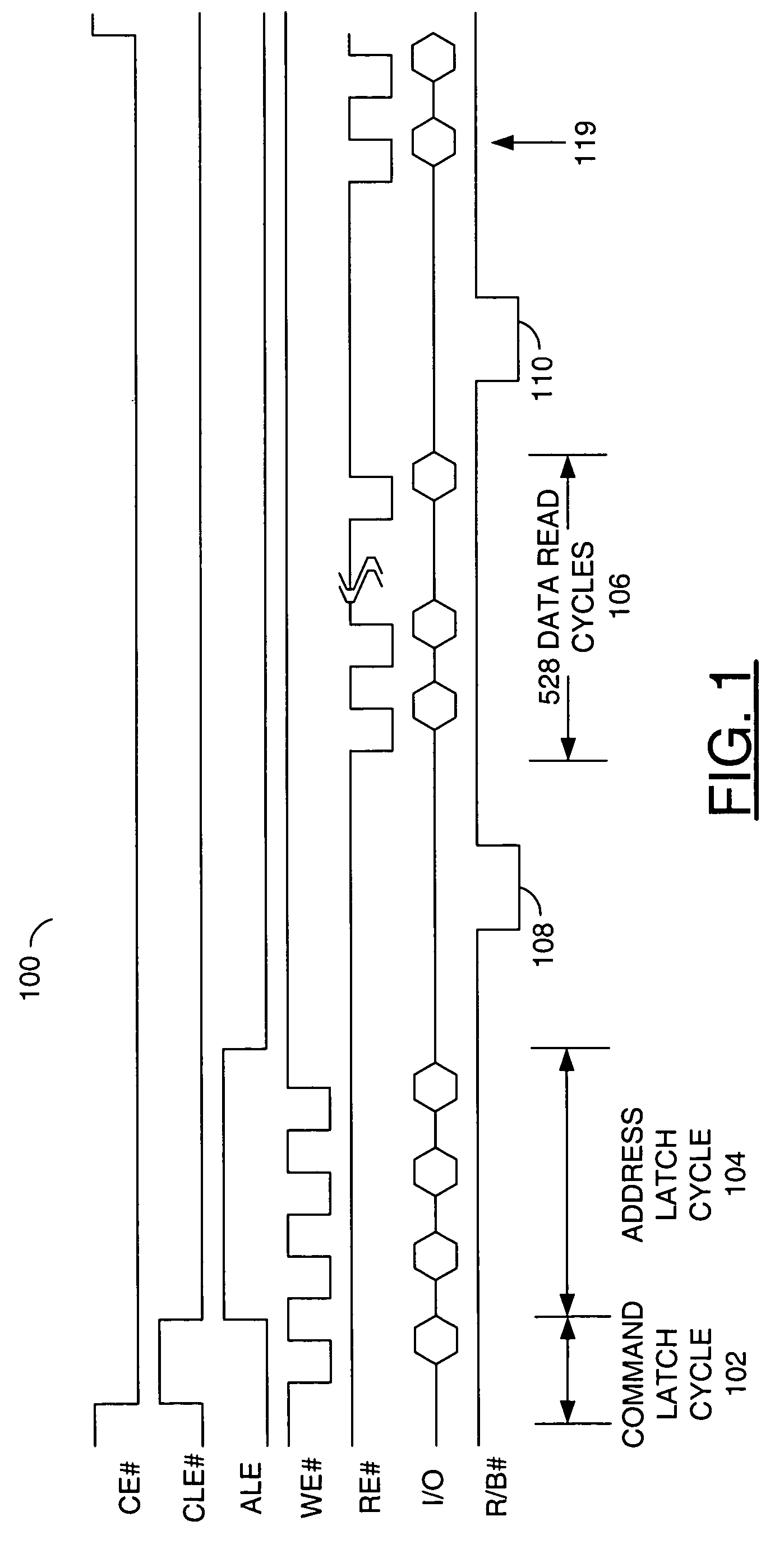
[0017] Communications through a NAND-Flash interface generally involve several parameters: (i) a data bus width parameter, (ii) a page size parameter, (iii) an address number parameter indicating a number of address cycles used to read data, (iv) a r...


PUM


Abstract

A method for automatically detecting a plurality of parameters for a NAND-Flash memory. A first step of the method may include generating a plurality of address cycles for the NAND-Flash memory. A second step may set an address number parameter of the parameters based on (i) a first number of the address cycles generated and (ii) a status signal generated by the NAND-Flash memory responsive to the address cycles. A third step generally includes generating at least one read cycle for the NAND-Flash memory after determining the address number parameter. A fourth step may set a page size parameter of the parameters based on (i) a second number of the read cycles generated and (ii) the status signal further responsive to the read cycles.

Description


Claims


Application Information

Patent Timeline
Owner AVAGO TECH INT SALES PTE LTD
Why Eureka
Try Eureka