

Photo detector package
a detector package and detector technology, applied in the field of detector packages, can solve problems such as significant measuring errors, and achieve the effect of ensuring measuring accuracy
- Summary
- Abstract
- Description
- Claims
- Application Information
AI Technical Summary
Benefits of technology
Problems solved by technology
Method used
Image

Examples
first embodiment
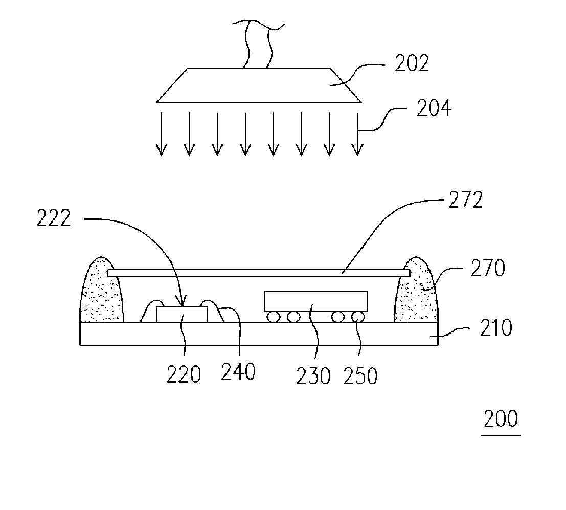
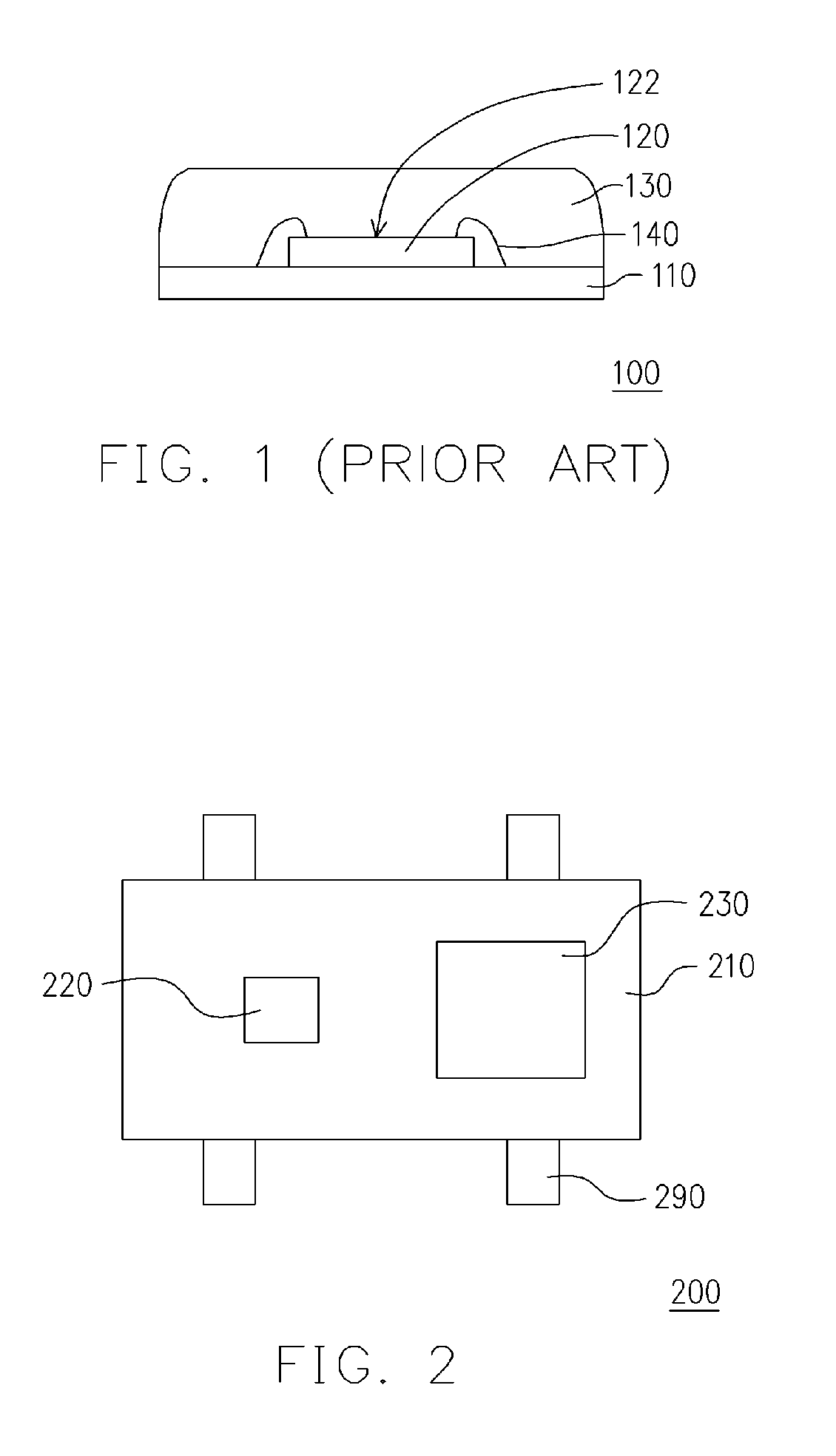
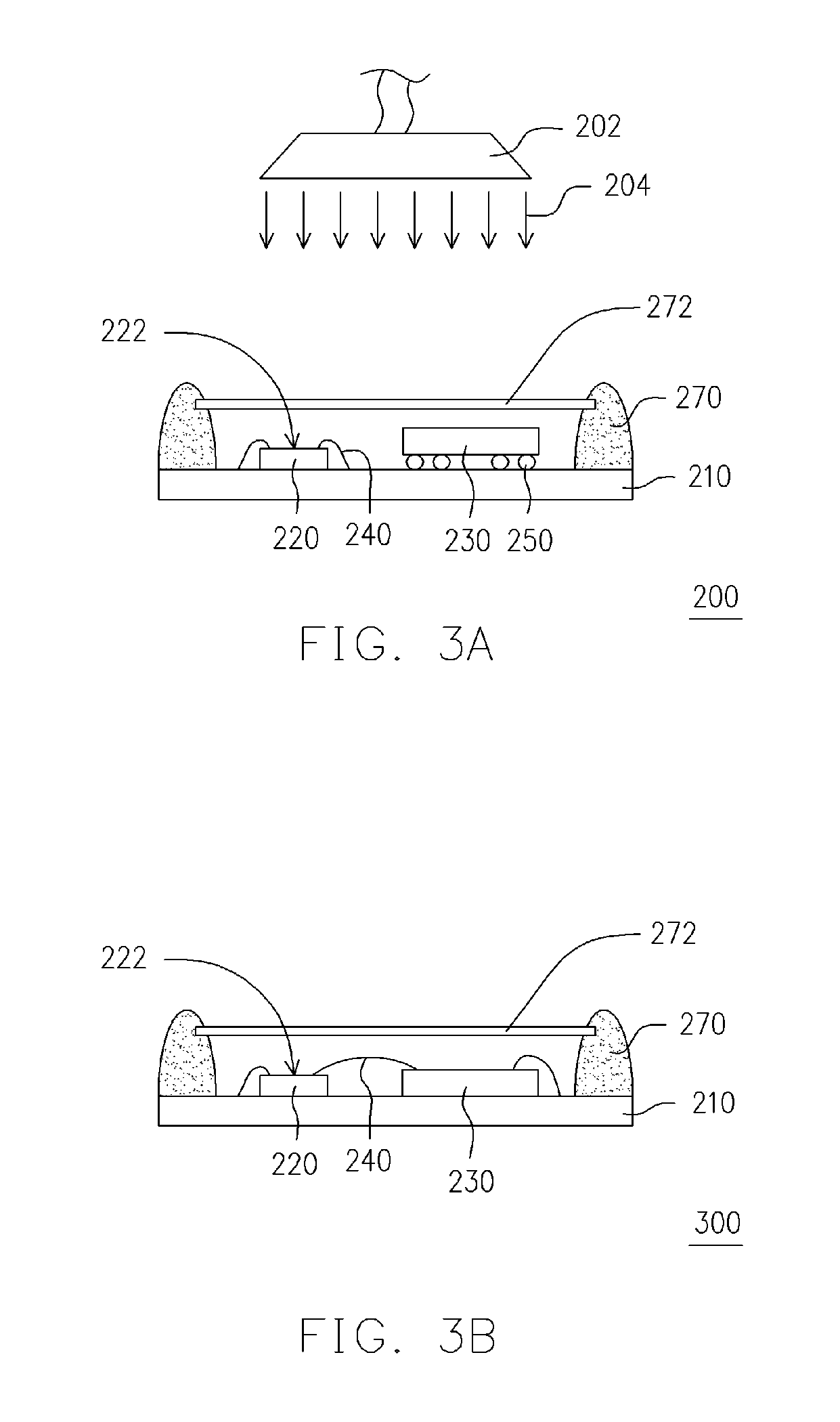
[0044]FIG. 2 is a perspective view of the photo detector package according to the present invention and FIG. 3A is a sectional view of the photo detector package shown in FIG. 2. Referring to FIG. 2 and FIG. 3A, the photo detector package 200 of the present invention includes a carrier 210, a photo sensor 220 and a calibration module 230. The calibration module 230 is disposed on the carrier 210 and electrically connected to the photo sensor 220 by the carrier 210. Moreover, the photo detector package 200 may further includes a plurality of external terminals 290, such as pins, contact pads, bumps or other types of contacts. The external terminals 290 are electrically connected to the photo sensor 220 and the calibration module 230 by the carrier 210.
[0045] In an embodiment of the present invention, the carrier 210 may be, for example, a circuit board, a packing substrate or a leadframe. The photo sensor 220 having an active surface 222 is disposed on the carrier and may be an ultra...
second embodiment
[0064] In conclusion, a photo sensor and a calibration module of a photo detector package are packaged together in the present invention, and after the photo detector package is calibrated by a calibration light source; a memory of a calibration module records the intensity of calibration light and a calibration signal into the memory; during measuring the intensity of light source to be measured, a judging processor compares a signal to be measured with the calibration signal and outputs a parameter representing the intensity of light to be measured to an image output module. Therefore, the photo detector package of the present invention can improve measuring accuracy of the intensity of light source during the measurement of the intensity of light source to be measured. Moreover, in the photo detector package of the present invention, the photo sensor stacks on the calibration module, so that the carrying area of the carrier of the photo detector package can be reduced.
PUM
 Abstract
Description
Claims
Application Information