Distance-measuring imaging device and solid-state imaging device

Active Publication Date: 2018-05-31
PANASONIC SEMICON SOLUTIONS CO LTD
View PDF6 Cites 3 Cited by
  • Summary
  • Abstract
  • Description
  • Claims
  • Application Information

AI Technical Summary

Benefits of technology

[0010]With a distance-measuring imaging device, etc. according to the present disclosure, it is possible to maintain distance measure

Problems solved by technology

The structure in Japanese Unexamined Patent Application Publication No. 2013-538342 thus has a pr

Method used


Image

  • Distance-measuring imaging device and solid-state imaging device
  • Distance-measuring imaging device and solid-state imaging device
  • Distance-measuring imaging device and solid-state imaging device

Examples


embodiment 1

(Variation of Embodiment 1)

[0084]The solid-state imager is not limited to a CCD image sensor. The same distance-measuring imaging device can be achieved even when any other solid-state imaging element (image sensor) such as a complementary metal-oxide semiconductor (CMOS) image sensor (CMOS solid-state imaging element) is used in view of other requirements of a distance-measuring imaging device.

[0085]FIG. 7 is a functional block diagram illustrating an example of the schematic structure of such distance-measuring imaging device 100A. Distance-measuring imaging device 100A illustrated in the drawing is similar to the distance-measuring imaging device in Embodiment 1, but includes solid-state imager 2A and timing generator 4A (controller) instead of solid-state imager 2 and drive controller 4.

[0086]Solid-state imager 2A includes a CMOS solid-state imaging element. In this variation, solid-state imager 2A is included in one chip together with timing generator 4A and TOF calculator 3 as...

embodiment 2

[0087]A distance-measuring imaging device according to Embodiment 2 is described below with reference to drawings. The following description mainly focuses on the differences from Embodiment 1.

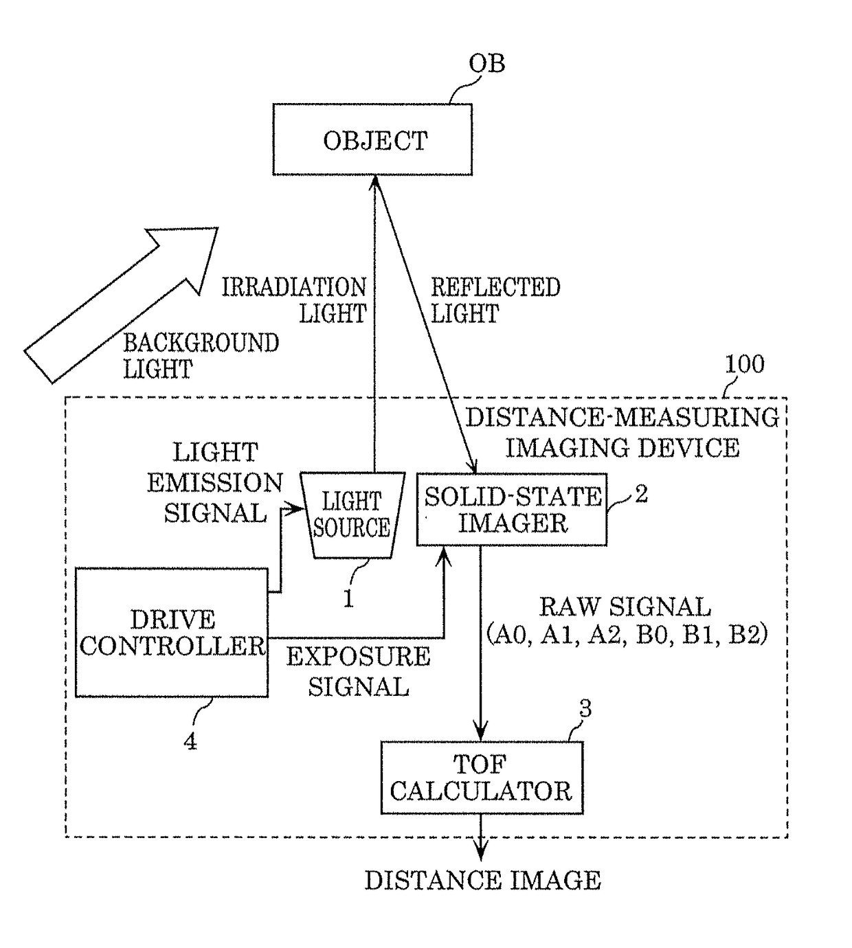
[0088]FIG. 8 is a functional block diagram illustrating an example of the schematic structure of distance-measuring imaging device 200 according to Embodiment 2. The drawing also illustrates object OB. Distance-measuring imaging device 200 measures the distance from distance-measuring imaging device 200 to object OB.

[0089]The difference of distance-measuring imaging device 200 illustrated in the drawing from distance-measuring imaging device 100 illustrated in FIG. 1 is that TOF calculator 203 calculates exposure amount B0 detected by BO exposure control and exposure amount B2 detected by B2 exposure control from the exposure amount obtained according to exposure signal group A.

[0090]The operation (driving method) of distance-measuring imaging device 200 in this embodiment is described below.

[...


PUM


Abstract

A distance-measuring imaging device includes: a drive controller that outputs a light emission signal and an exposure signal; a light source; a solid-state imager that performs exposure to reflected light; and a TOF calculator that calculates a distance to an object using an imaging signal. The drive controller: cyclically outputs a first exposure signal group in which, before an exposure period of one exposure signal ends, an exposure period of at least one other exposure signal starts; and outputs a second exposure signal group having a dead zone period during which all exposure signals are in a non-exposure period. The TOF calculator calculates a first distance value using a first imaging signal obtained according to the first exposure signal group, calculates a second distance value using a second imaging signal obtained according to the second exposure signal group, and calculates the distance based on the first and second distance values.

Description

CROSS REFERENCE TO RELATED APPLICATIONS[0001]This application is a U.S. continuation application of PCT International Patent Application Number PCT / JP2016 / 002485 filed on May 23, 2016, claiming the benefit of priority of Japanese Patent Application Number 2015-152764 filed on Jul. 31, 2015, the entire contents of which are hereby incorporated by reference.BACKGROUND1. Technical Field[0002]The present disclosure relates to a distance-measuring imaging device and a solid-state imaging device used in the distance-measuring imaging device.2. Description of the Related Art[0003]Of a plurality of methods for detecting an object, a time of flight (TOF) method of measuring a distance using a time of flight during which light travels to and from a measurement object (object) is known.[0004]In the TOF method, the distance measurement accuracy (distance measurement resolution) and the distance range depend on the frequency of irradiation light (the length of a light emission period). When the ...

Claims


Application Information

Patent Timeline
IPC IPC(8): G01S17/10H04N5/355G01S17/89G01S17/894G01S7/4865H04N5/372H04N5/374
CPCG01S17/10H04N5/35581G01S17/89H04N5/372H04N5/374G01S7/4865H01L27/14643H01L27/14831G01S17/894H04N25/533H04N25/71H04N25/76H04N25/589
Inventor KISHIMOTO, MASAYATAKANO, HARUKA
Owner PANASONIC SEMICON SOLUTIONS CO LTD
Why Eureka
Try Eureka