
Analog-to-digital conversion in pixel arrays

a technology of pixel arrays and analog to digital conversion, applied in the field of analog-to-digital conversion, can solve the problems of low conversion accuracy, high cost in terms of area and layout in semiconductor devices, and limited rate at which adc can operate, so as to improve the accuracy of accumulated values and reduce conversion time

Active Publication Date: 2011-02-01
CMOSIS
View PDF14 Cites 69 Cited by
  • Summary
  • Abstract
  • Description
  • Claims
  • Application Information

AI Technical Summary

Benefits of technology

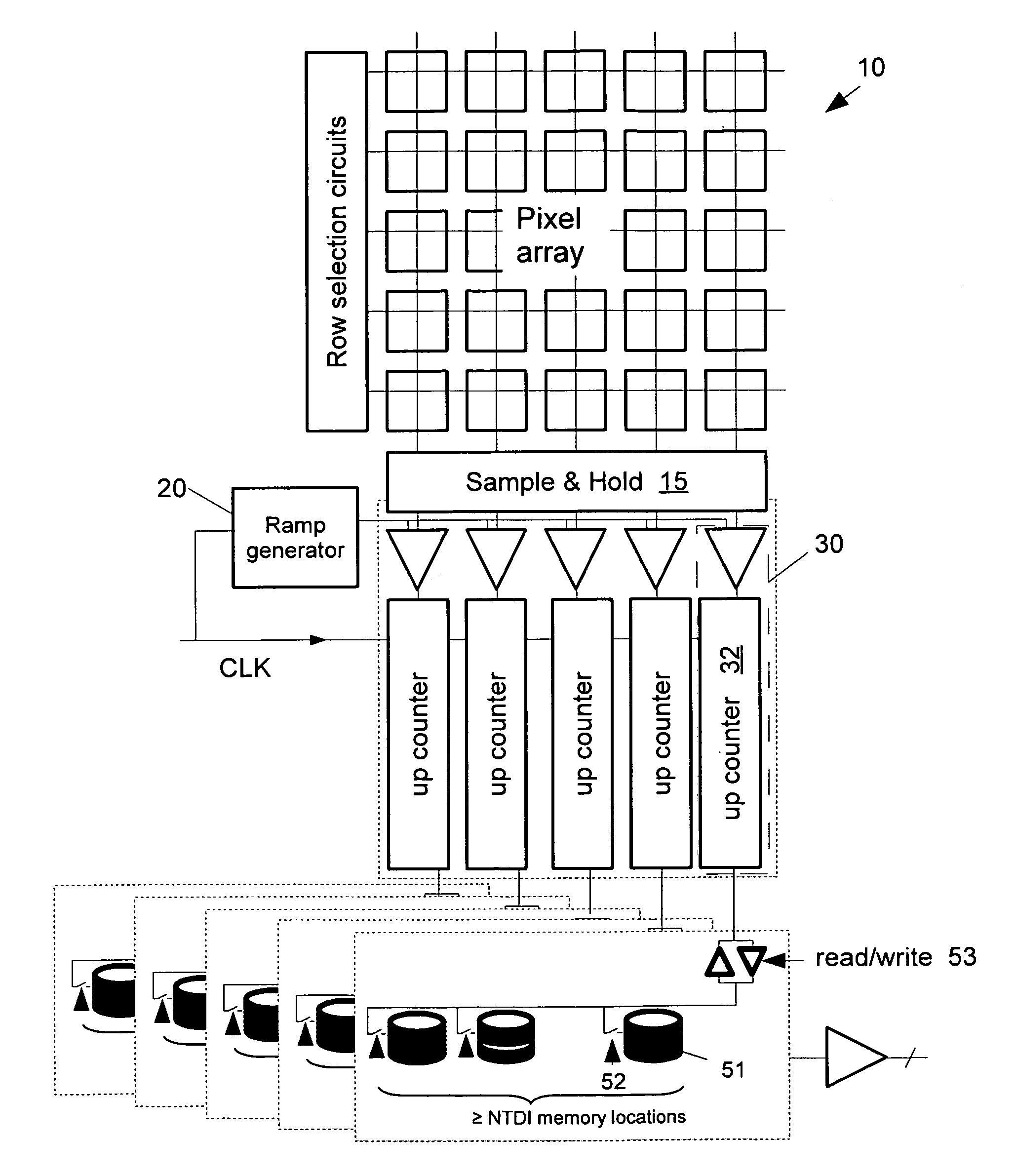
[0015]This aspect of the invention can have an advantage of avoiding the need to distribute a counter signal across multiple ADC units, which improves the accuracy of the accumulated value. It can also avoid the need for counter direction changing circuitry as each counter is only required to count in a single direction.
[0016]The analog-to-digital converter performs the conversion during a conversion cycle. The conversion cycle can make use of a ramp signal having two cycles, or just a single cycle. The use of a single ramp cycle can reduce the conversion time as both of the analog signals are compared with the same cycle of the ramp signal. The comparison of the first and second analog signals with the ramp signal can occur concurrently or sequentially during the ramp signal. The control stage can use an intentional offset during the comparisons of the first and second analog signals with the ramp signal.
[0032]This aspect of the invention is particularly advantageous in Time Delay and Integration (TDI) applications and any application where multiple values need to be accumulated. Initialising the counter in the ADC to the previously accumulated value allows accumulation without the need for a separate adder, which can provide a considerable saving in semiconductor area and layout.
[0034]Advantageously, the processing unit monitors the accumulated digital value and determines if any further processing operations should occur. This determination can be based on the current accumulated exposure level. Operating in this manner makes it possible to prevent saturation of image elements, before saturation occurs. The determination can be made independently for each accumulated element of the image.
[0042]This aspect of the invention can have an advantage of increasing speed of conversion in the ADC without requiring a high speed clock signal.
[0047]Features of the first, second and third aspects of the present invention can be combined with one another. For example, the first aspect of the invention can make use of the features of the third aspect of the invention to improve conversion speed.

Problems solved by technology

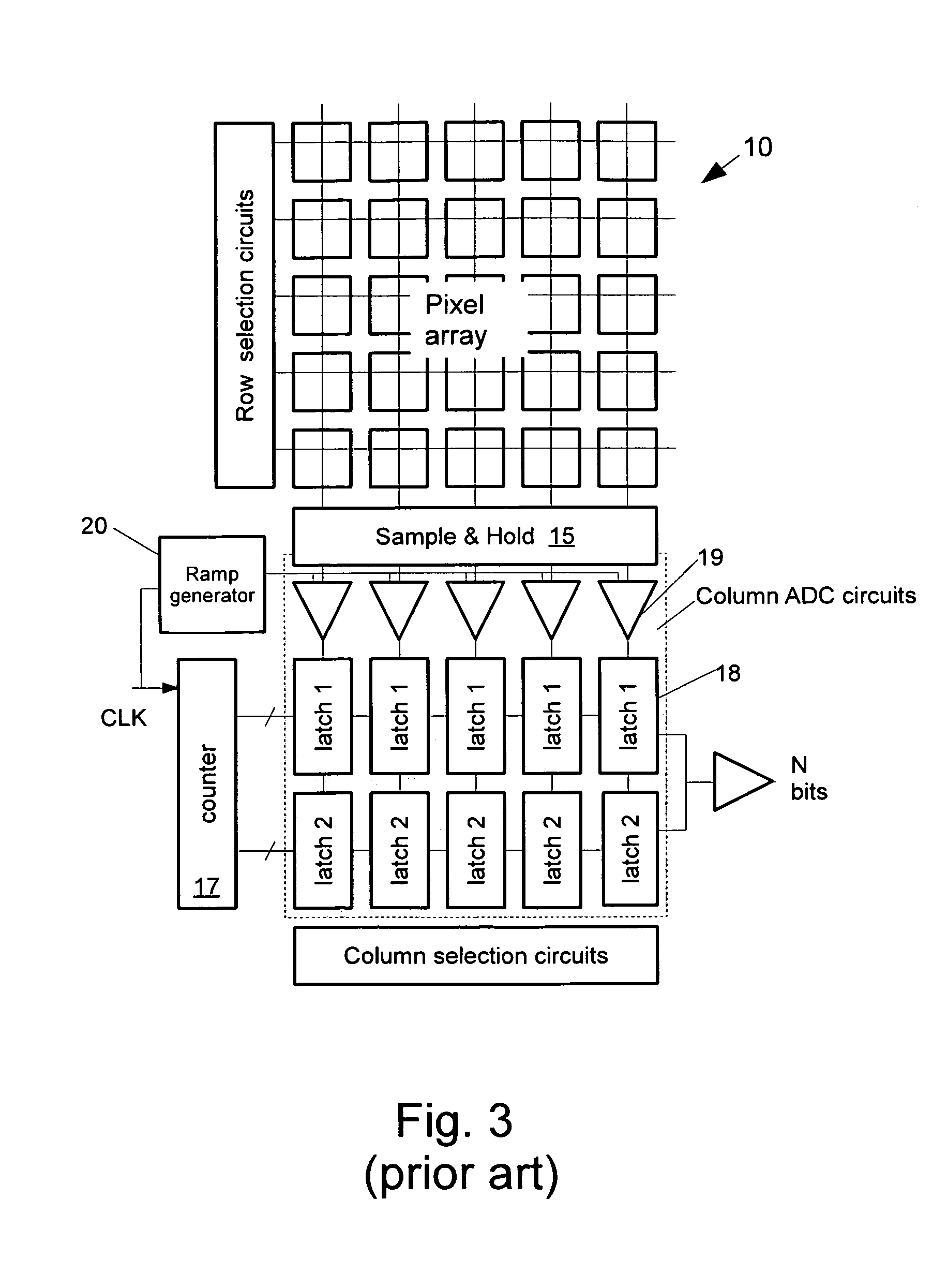
Column-to-column variations of clock skew, which cause conversion error, are generated when a high-speed clock is used.
This can be expensive in terms of area and layout in a semiconductor device.
The rate at which the ADC can operate is limited by several constraints.
In practice, there is a limit to the clock frequency that can be achieved.

Method used


Image

  • Analog-to-digital conversion in pixel arrays
  • Analog-to-digital conversion in pixel arrays
  • Analog-to-digital conversion in pixel arrays

Examples


Embodiment Construction

[0069]The present invention will be described with respect to particular embodiments and with reference to certain drawings but the invention is not limited thereto but only by the claims. The drawings described are only schematic and are non-limiting. In the drawings, the size of some of the elements may be exaggerated and not drawn on scale for illustrative purposes. Where the term “comprising” is used in the present description and claims, it does not exclude other elements or steps. Furthermore, the terms first, second, third and the like in the description and in the claims, are used for distinguishing between similar elements and not necessarily for describing a sequential or chronological order. It is to be understood that the terms so used are interchangeable under appropriate circumstances and that the embodiments of the invention described herein are capable of operation in other sequences than described or illustrated herein.

[0070]Throughout this specification, it should ...


PUM


Abstract

An analog-to-digital converter (ADC) generates an output digital value equivalent to the difference between two analog signal values. The ADC 30 receives a first analog signal level, a second analog signal level and a ramp signal. A counter 32 is operable to count in a single direction. A control stage is arranged to enable the counter 32 based on a comparison 19 of the ramp signal with the first analog signal and the second analog signal. A digital value accumulated by the counter during a period when it is enabled forms the output. The ADC can perform the conversion during a single cycle of the ramp signal. The counter 32 can be loaded with a starting digital value representing an exposure level accumulated during a previous exposure period. Techniques are described for reducing the conversion time.

Description

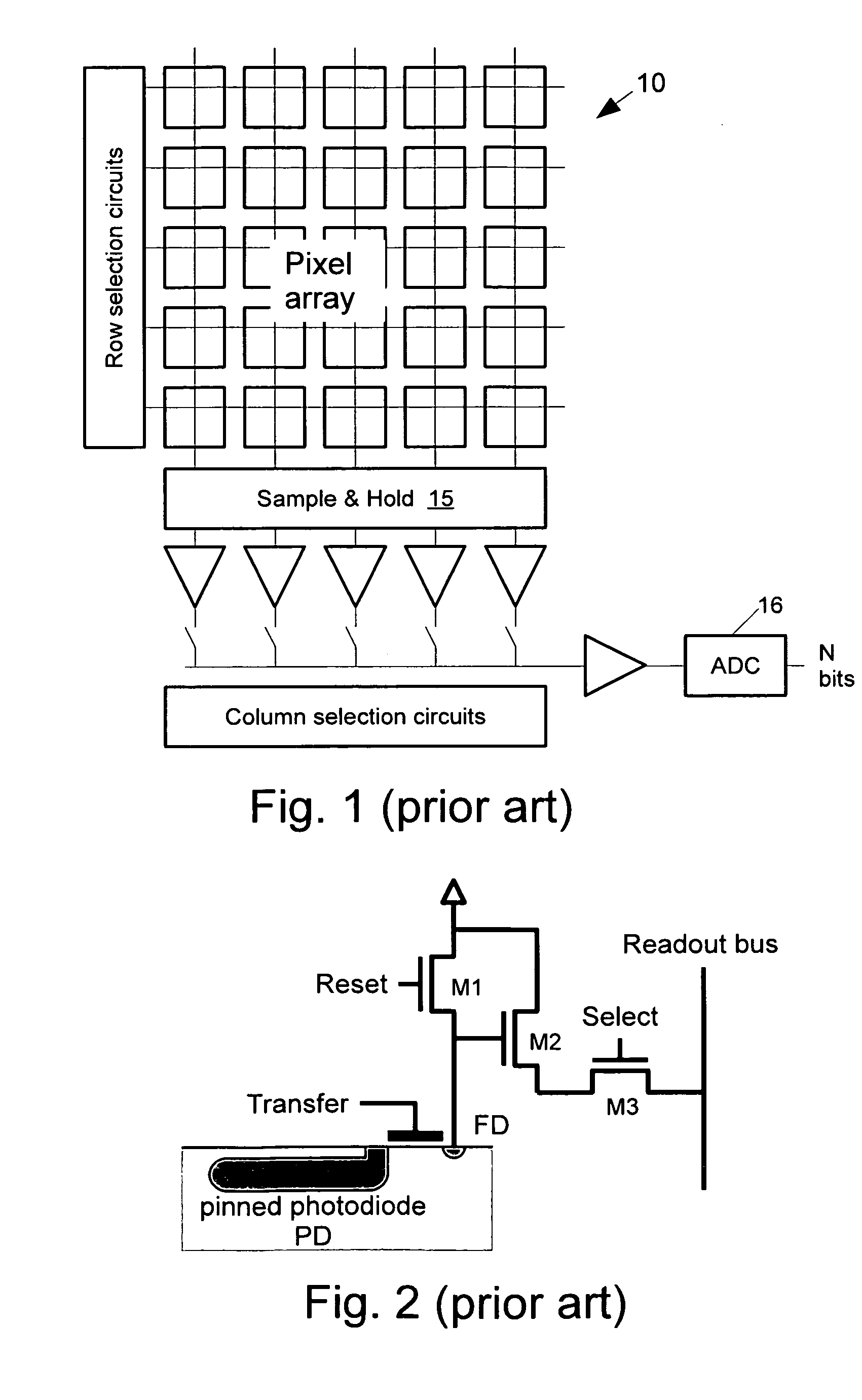
FIELD OF THE INVENTION[0001]This invention relates to analog-to-digital conversion which can be used, for example, in processing signals output from a pixel array.BACKGROUND TO THE INVENTION[0002]Imaging sensors comprise an array of unit elements (pixels). The array of pixels is exposed to radiation during an exposure period and, subsequently, the signal value of each pixel is read from the array. The array can be a one dimensional array (linear sensor) or a two dimensional array (area array) with pixels arranged in rows and columns.[0003]FIG. 1 shows the architecture of a CMOS imaging sensor. Impinging photons are converted into charges in the pixel array and are accumulated during a certain integration period. Typically, the pixels are selected row by row for readout of their signals. A typical 4T pixel is shown in FIG. 2. The pixel includes a photodiode PD, a transfer gate to transfer the charges in the photodiode to the floating diffusion FD, a reset transistor M1, a source foll...

Claims


Application Information

Patent Timeline
Patent Type & Authority Patents(United States)
IPC IPC(8): H03M1/56
CPCH03M1/1019H04N5/3575H03M1/123H03M1/1295H03M1/56H03M1/203H04N25/616
Inventor BOGAERTS, JAN
Owner CMOSIS
Learn More