Enhanced simultaneous multi-spot inspection and imaging
a multi-spot inspection and imaging technology, applied in the field of surface inspection, can solve the problems of increasing the amount of time required to scan over the entire surface using the smaller spot, increasing the amount of scan time, and increasing the difficulty of implementation of the 45-degree angle design
- Summary
- Abstract
- Description
- Claims
- Application Information
AI Technical Summary
Problems solved by technology
Method used
Image
Examples
Embodiment Construction
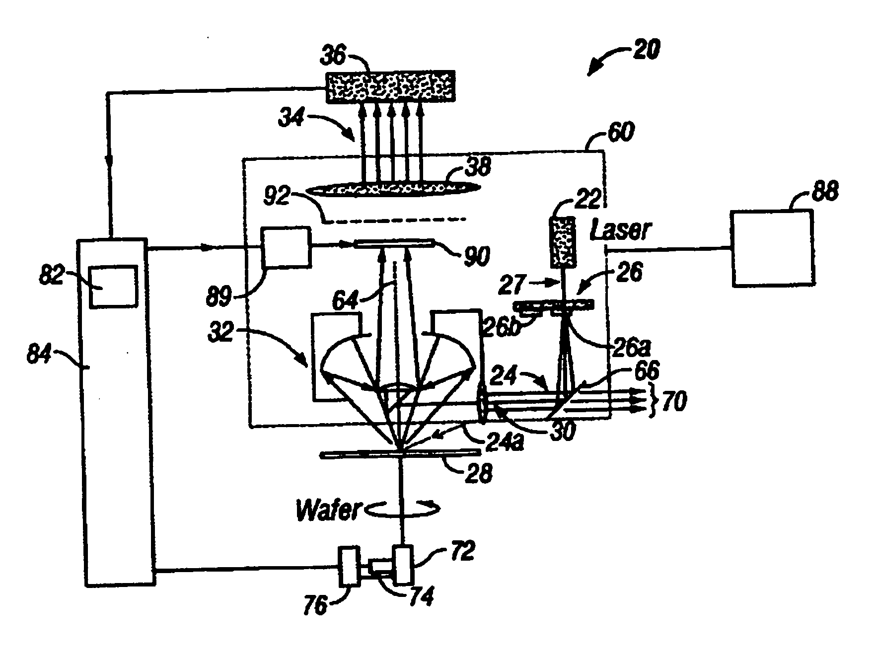
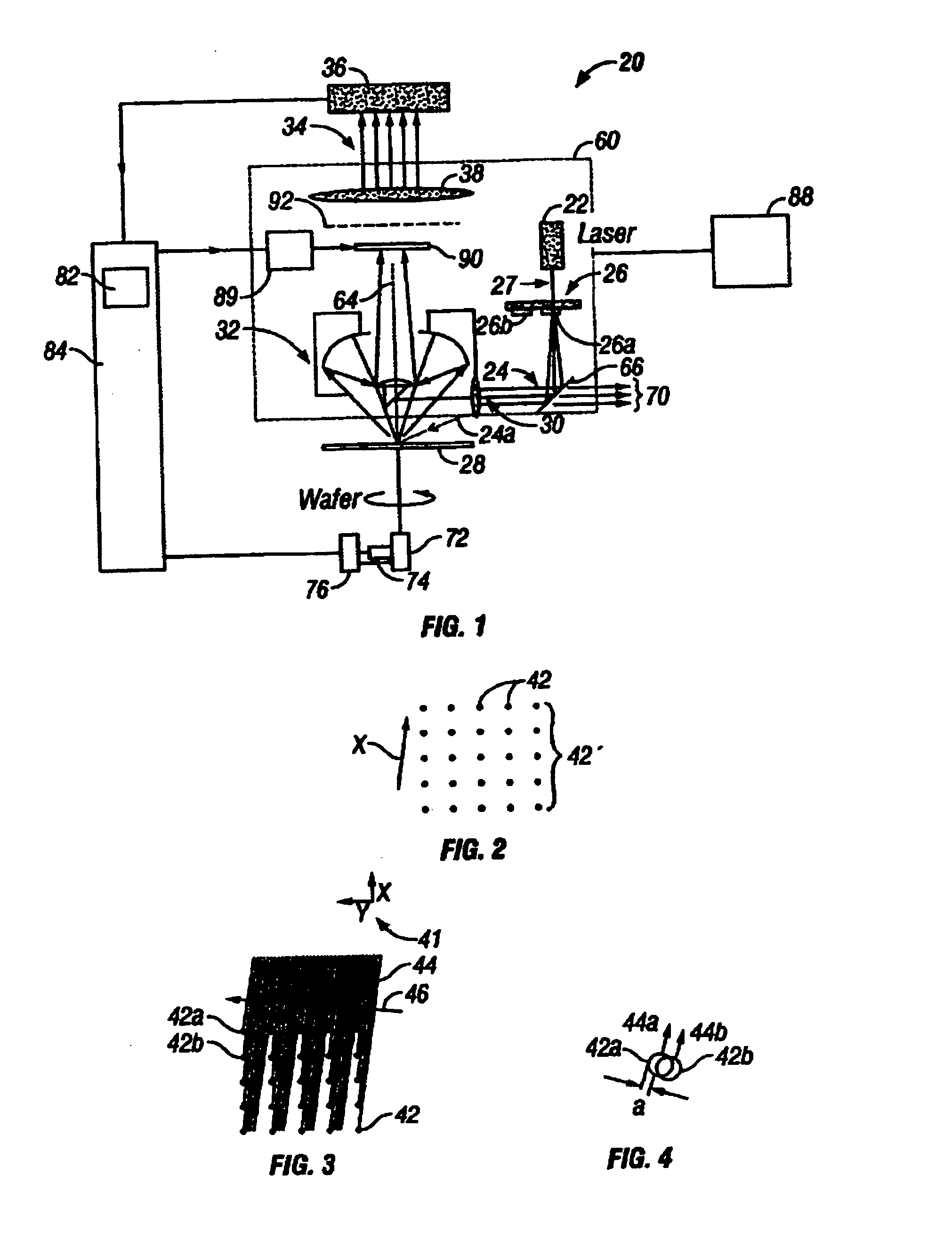
[0025] The costs associated with dark-field pattern inspection have increased steadily with enhanced performance. As semiconductor fabrication approaches finer design rule and resolution, the complexity of inspection tasks has increased dramatically, which, in turn, increases the complexity and costs of the optical front end of the inspection tool and of detection electronics. Furthermore, the variety of situations calling for optical inspection means that a versatile optical inspection tool should be compact, have a small foot print and be rugged so that it is less sensitive to vibrations, and integratable with semiconductor processing equipment. Preferably, the system can be used for inspecting surfaces with diffracting patterns thereon such as patterned wafers, as well as surfaces without such patterns such as unpatterned semiconductor wafers. The present design enables faster and more sensitive inspection to be performed at a reasonable cost.
[0026] The elements of the optical f...
PUM
 Abstract
Description
Claims
Application Information


