Local multilayered metallization

a technology of metallization and multi-layers, applied in the direction of semiconductor devices, electrical equipment, semiconductor/solid-state device details, etc., can solve the problems of increasing the complexity of manufacturing operations and failure rate of manufactured circuits, high cost, and high cost of solutions

Inactive Publication Date: 2006-09-07
MICRON TECH INC
View PDF51 Cites 15 Cited by
  • Summary
  • Abstract
  • Description
  • Claims
  • Application Information

AI Technical Summary

Problems solved by technology

Unfortunately, when copper and copper alloy pads are wire-bonded to a highly conductive wire, such as a gold, using current state-of-the-art wire-bonding processes, the resulting copper and gold bonds or copper alloy and gold bonds are not as reliable as aluminum and gold bonds or aluminum alloy and gold bonds used in the prior art.
Unfortunately, this solution has several problems.
Second, the extra processing steps increase the complexity of the manufacturing operation and the failure rate of the manufactured circuits.
Third, the solution is expensive, since it requires more materials, masking steps, and time than the prior art processes to manufacture the integrated circuit.

Method used


Image

  • Local multilayered metallization
  • Local multilayered metallization
  • Local multilayered metallization

Examples


Embodiment Construction

[0013] The above mentioned problems with integrated circuit metallization and other problems are addressed by the present invention and will be understood by reading and studying the following specification.

[0014] In the following detailed description of the preferred embodiments, reference is made to the accompanying drawings which form a part hereof, and in which is shown by way of illustration specific preferred embodiments in which the invention may be practiced. These embodiments are described in sufficient detail to enable those skilled in the art to practice the invention, and it is to be understood that other embodiments may be utilized and that logical, mechanical and electrical changes may be made without departing from the spirit and scope of the present invention. The following detailed description is, therefore, not to be taken in a limiting sense, and the scope of the present invention is defined only by the appended claims.

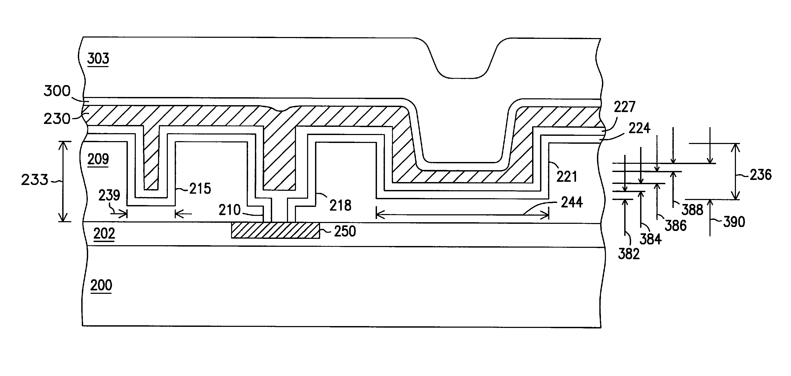
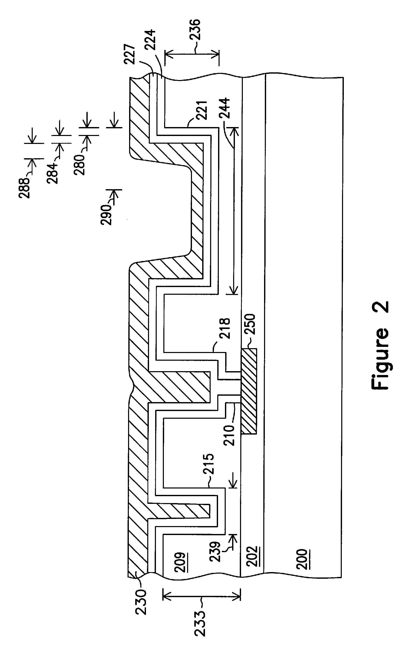
[0015]FIG. 2 is a cross-sectional side view...


PUM

PropertyMeasurementUnit
thicknessaaaaaaaaaa
thicknessaaaaaaaaaa
thicknessaaaaaaaaaa

Abstract

An interconnect comprises a trench and a number of metal layers above the trench. The trench has a depth and a width. The depth is greater than a critical depth, and the number of metal layers is a function of the width. In an alternate embodiment, a metallization structure having a trench including a metal layer and a second trench including a plurality of metal layers coupled to the metal layer is disclosed. The metal layer is highly conductive, and at least one of the plurality of metal layers is a metal layer that is capable of being reliably wire-bonded to a gold wire. The trench is narrower than the second trench, and at least one of the plurality of metal layers is copper or a copper alloy.

Description

RELATED APPLICATIONS [0001] This application is a Divisional of U.S. application Ser. No. 10 / 931,357, filed Aug. 31, 2004, which is a Divisional of U.S. application Ser. No. 09 / 388,567, filed Sep. 2, 1999, both of which are incorporated herein by reference.FIELD OF THE INVENTION [0002] This invention relates to the field of integrated circuit manufacturing, and more particularly to metallization in integrated circuit manufacturing. BACKGROUND OF THE INVENTION [0003] Copper and copper alloys are often substituted for the more traditional aluminum and aluminum alloys as the primary signal and power carrying conductive structures in integrated circuits. Unfortunately, when copper and copper alloy pads are wire-bonded to a highly conductive wire, such as a gold, using current state-of-the-art wire-bonding processes, the resulting copper and gold bonds or copper alloy and gold bonds are not as reliable as aluminum and gold bonds or aluminum alloy and gold bonds used in the prior art. [00...

Claims


Application Information

Patent Timeline
Patent Type & Authority Applications(United States)
IPC IPC(8): H01L21/44H01L21/4763H01L21/768H01L23/485H01L23/528H01L23/532
CPCH01L21/76816H01L21/76843H01L21/76877H01L23/5283H01L23/53238H01L24/03H01L24/05H01L24/06H01L24/45H01L24/48H01L2224/04042H01L2224/05006H01L2224/05073H01L2224/05147H01L2224/05166H01L2224/05181H01L2224/05187H01L2224/05546H01L2224/05567H01L2224/05624H01L2224/45124H01L2224/45144H01L2224/48463H01L2224/48624H01L2924/01013H01L2924/01014H01L2924/01022H01L2924/01029H01L2924/01031H01L2924/01032H01L2924/0105H01L2924/01073H01L2924/01074H01L2924/01079H01L2924/01322H01L2924/04941H01L2924/04953H01L2924/14H01L2924/19041H01L2924/19043H01L2924/30105H01L2924/01033H01L2224/48724H01L2924/0002H01L2224/02166H01L2924/00014H01L2924/00H01L2224/05552H01L2224/023H01L2224/02126H01L2924/0001
Inventor RHODES, HOWARD E.
Owner MICRON TECH INC
Why Eureka
Try Eureka