Method for MCP packaging for balanced performance

a technology of balanced performance and mcp, applied in the field of multi-chip modules, can solve the problems of inferior performance of the upper ic and different performance of the different ics

Inactive Publication Date: 2006-09-14
INFINEON TECH AG
View PDF45 Cites 23 Cited by
  • Summary
  • Abstract
  • Description
  • Claims
  • Application Information

AI Technical Summary

Benefits of technology

[0015] Still another embodiment provides a multi-chip package having a substrate defining a first substrate surface and comprising a plurality of contact areas. A first memory chip is in a face-up position over the substrate so that a first surface of the first memory chip and the first substrate surface are in facing relationship with respect to one another and a second surface of the first memory chip faces away from the substrate; wherein the first memory chip comprises a redistribution layer comprising a plurality of inner contacts coupled to a plurality of outer pads via respective traces; the inner pads being located in an inner region of the second surface and the outer pads being located being located in an outer region of the second surface; a second memory chip having the same dimensions as the first memory chip and disposed over at least a portion of the first integrated circuit so that the second surface of the first memory chip is facing a first surface of the second memory chip, wherein the second memory chip comprises a plurality of pads; and wherein the second memory chip is sufficiently laterally offset relative to the first memory chip to expose the outer region and substantially prevent the plurality of outer pads from being covered by the second memory chip. Bond wires couple the outer pads of the first memory chip and the plurality of pads of the second memory chip to the plurality of contact areas.

Problems solved by technology

However, one problem that occurs with wire bonding in MCP is that the various ICs perform differently relative to one another due to the different bond wire lengths.
As a result, there is a RLC value difference resulting in an inferior performance of the upper IC 110 relative to the performance of the lower IC 120.

Method used


Image

  • Method for MCP packaging for balanced performance
  • Method for MCP packaging for balanced performance
  • Method for MCP packaging for balanced performance

Examples


Embodiment Construction

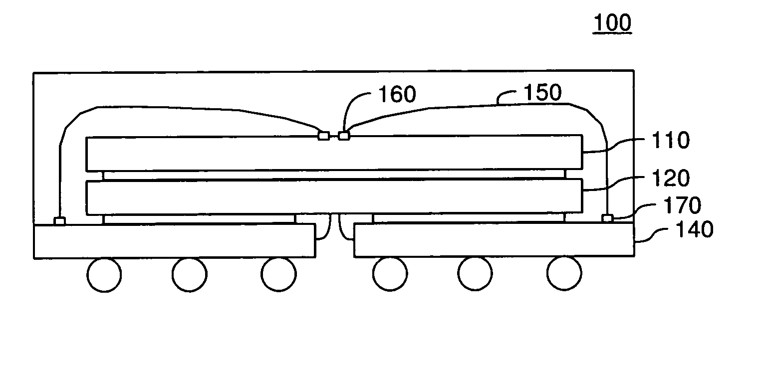
[0022] Embodiments of the invention generally provide balanced packaging methods and balanced packages. In one embodiment, the invention offers an alternative packaging method that reduces, or eliminates, the RLC difference between two or more dies in a MCP. In addition, the capacitive loading would be relatively more balanced between the dies; that is, one of the dies will not have a much greater capacitive load than another die in the package.

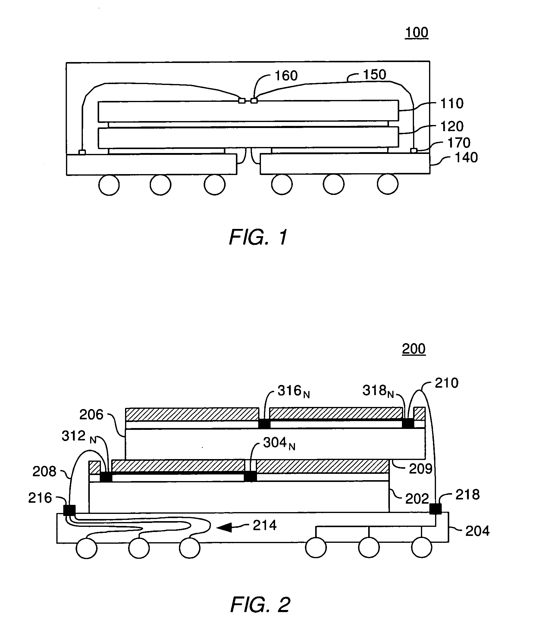
[0023] In a first embodiment, a MCP includes face-up dies, i.e., the pads on the dies face away from a substrate. FIG. 2 shows an MCP 200 with such an arrangement. Specifically, a bottom die 202 is disposed over a substrate 204 and is in a face-up orientation, meaning contact pads (316, 318) formed on an upper surface of the bottom die 202 are facing away from the substrate 204. A top die 206 is disposed over the bottom die 202 and is also in a face-up position meaning contact pads (304, 312) formed on an upper surface of the top die 206 are...


PUM


Abstract

Embodiments of the invention generally provide methods and apparatus for constructing multi chip packages having balance performance as between the various integrated circuits in a stack. In one embodiment, contacts on an outer surface of a first pad are “redistributed” from one area of the outer surface to another area of the first pad (e.g., to a different area of the outer surface). A second chip is adjacent to, and laterally offset with, the first chip, thereby exposing the redistributed contacts of the first chip.

Description

CROSS-REFERENCE TO RELATED APPLICATIONS [0001] This application is related to U.S. patent application Ser. No. 11 / 039,293, Attorney Docket No. INFN / 0097 (2004P53356US), entitled SIGNAL REDISTRIBUTION USING BRIDGE LAYER FOR MULTICHIP MODULE, filed Jan. 20, 2005, by Thoai Thai Le et al., and U.S. patent application Ser. No. 11 / 079,620, Attorney Docket No. INFN / WB0157, entitled METHOD FOR PRODUCING CHIP STACKS AND CHIP STACKS FORMED BY INTEGRATED DEVICES, filed Mar. 14, 2005, by Harald Gross. Each of the aforementioned related patent applications is herein incorporated by reference in its entirety.BACKGROUND OF THE INVENTION [0002] 1. Field of the Invention [0003] The invention generally relates to multichip modules (MCMs). [0004] 2. Description of the Related Art [0005] Many electronic applications require a set of integrated circuit (IC) chips that are packaged together, for example, on a common printed circuit (PC) board. For example, many applications call for a processor and some ...

Claims


Application Information

Patent Timeline
Patent Type & Authority Applications(United States)
IPC IPC(8): H01L23/02
CPCH01L23/3128H01L2924/19107H01L25/0657H01L25/50H01L2224/48091H01L2224/48227H01L2224/4824H01L2225/0651H01L2225/06517H01L2225/06555H01L2225/06562H01L2225/06586H01L2225/06593H01L2924/01078H01L2924/01079H01L2924/14H01L2924/15311H01L25/0652H01L2224/06136H01L2224/06135H01L2224/92247H01L2224/73265H01L2224/73215H01L2224/32225H01L2224/32145H01L2924/00014H01L2924/00H01L2924/00012H01L24/73
Inventor BARAKAT, FARIDNEGUSSU, PETROSLE, THOAI THAI
Owner INFINEON TECH AG
Why Eureka
Try Eureka