Processing apparatus and recording medium

a processing apparatus and recording medium technology, applied in the direction of electrical equipment, basic electric elements, semiconductor/solid-state device manufacturing, etc., can solve problems such as cracks or broken, and achieve the effects of preventing the breakage of the substrate, preventing the displacement of the substrate, and facilitating the detection of the chipping of the substra

Inactive Publication Date: 2006-09-28
TOKYO ELECTRON LTD
View PDF5 Cites 143 Cited by
  • Summary
  • Abstract
  • Description
  • Claims
  • Application Information

AI Technical Summary

Benefits of technology

[0013] The present invention was made in consideration of the above-described circumstances, and its object is to provide a processing apparatus and a recording medium that realize easy detection of chipping of a substrate which sometimes occurs when the processed substrate is carried and loaded on a substrate loading part of a temporary storage unit, and thus realizes the prevention of the breakage of the substrate in subsequent processes. It is another object of the present invention to provide a processing apparatus and a recording medium that realize easy detection of the displacement of a substrate occurring in a process chamber or on a transfer route.

Problems solved by technology

This involves the possibility that the wafer suffering the chipping is carried and put in the FOUP without any error detection and is cracked or broken in the subsequent processes.

Method used


Image

  • Processing apparatus and recording medium
  • Processing apparatus and recording medium
  • Processing apparatus and recording medium

Examples


Embodiment Construction

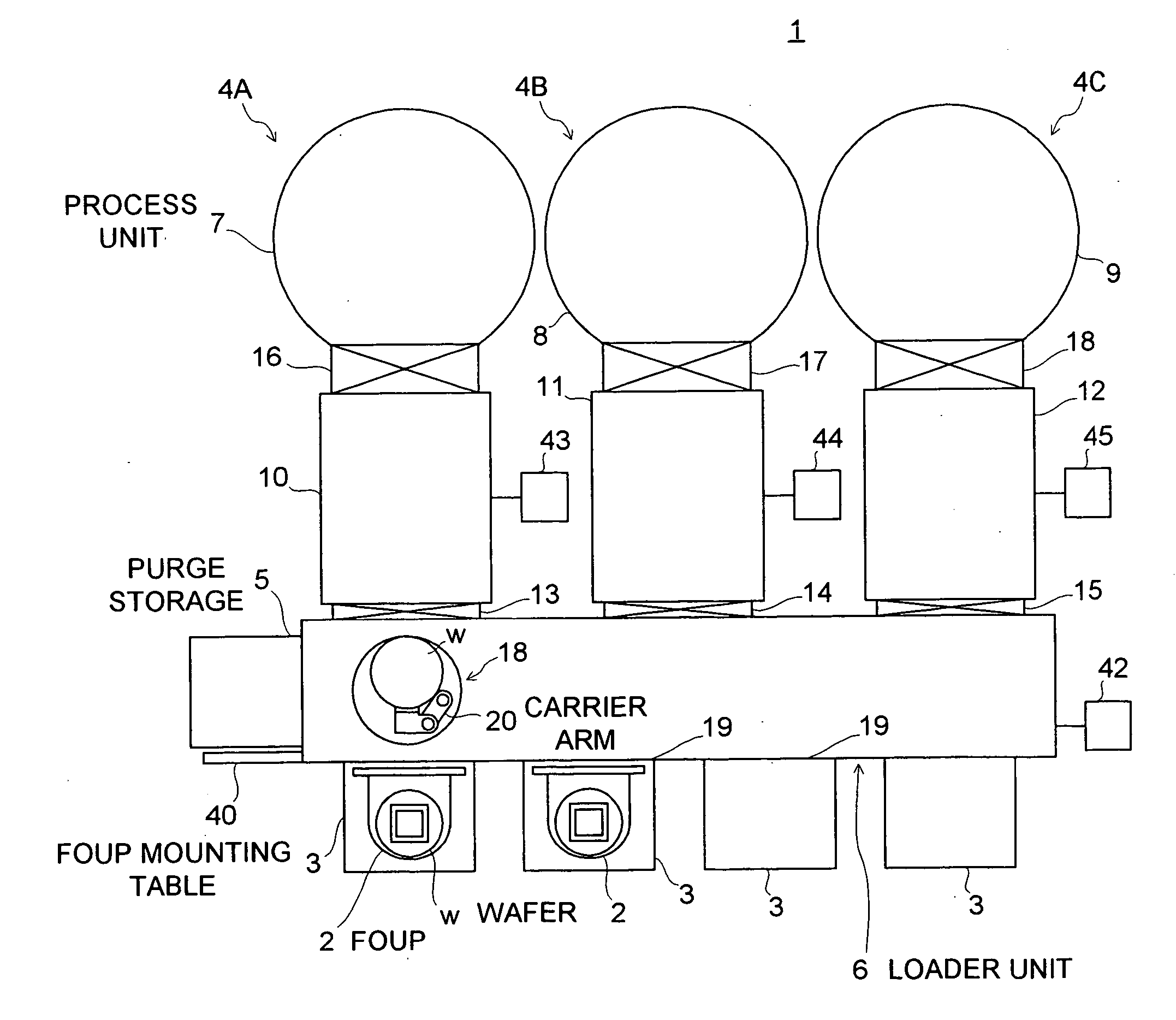
[0031] Hereinafter, the best mode for carrying out the present invention will be described with reference to the drawings. FIG. 1 is a plane view showing a rough structure of a processing apparatus according to an embodiment of the present invention.

[0032] In FIG. 1, 1 denotes a single-wafer processing apparatus in which semiconductor wafers (hereinafter referred to as wafers) W as substrates to be processed are carried and undergo predetermined processing one by one. The processing apparatus 1 includes: a plurality of, for example, four FOUP mounting tables 3 as mounting tables on which FOUPs 2 as carriage containers each containing a plurality of, for example, 25 wafers W are placed; three process ships 4A, 4B, 4C each including a process unit (process chamber) in which predetermined processing, for example, etching is applied to the wafer W; a purge storage 5 as a temporary storage unit temporarily storing the plural processed wafers W in multi-tiers; and a loader unit 6 being a...


PUM


Abstract

A processing apparatus includes: a mounting table on which a carriage container containing a plurality of substrates is placed; a process chamber in which predetermined processing is applied to the substrate; a temporary storage unit having a substrate loading part on which the plural processed substrates are loaded in multi-tiers; a transfer unit having a carrier arm carrying the substrate to/from the carriage container on the mounting table, the process chamber, and the temporary storage unit; a vibration sensor detecting vibration of the substrate loading part; and a control unit which compares a current detection value of the vibration sensor with a predetermined set value to judge whether or not the vibration is abnormal vibration and to stop the carrier arm when judging that the vibration is the abnormal vibration.

Description

CROSS-REFERENCE TO RELATED APPLICATION [0001] This application is based upon and claims the benefit of priority from the prior Japanese Patent Application No. 2005-090832, filed on Mar. 28, 2005; and the prior U.S. Patent Provisional Application No. 60 / 666,573, filed on Mar. 31, 2005; the entire contents which are incorporated herein by reference.BACKGROUND OF THE INVENTION [0002] 1. Field of the Invention [0003] The present invention relates to a processing apparatus and a recording medium, and more particularly, to an art of detecting chipping of a substrate. [0004] 2. Description of the Related Art [0005] The manufacture of a semiconductor device includes processes of applying various kinds of processing, for example, etching and so on to, for example, a semiconductor wafer (hereinafter referred to as a wafer) which is a substrate to be processed, and a processing apparatus is used for implementing these processes. The processing apparatus includes: a FOUP mounting table on which...

Claims


Application Information

Patent Timeline
Patent Type & Authority Applications(United States)
IPC IPC(8): H01T23/00
CPCH01L21/67167H01L21/67288H01L21/67742
Inventor WAKABAYASHI, SHINJI
Owner TOKYO ELECTRON LTD
Why Eureka
Try Eureka