IC package with prefabricated film capacitor

a film capacitor and ic package technology, applied in the field of integrated circuit packages, can solve the problems of difficult to achieve a thick film, difficult to achieve a sputtered film, and difficult to embed hi-k thin film into the substrate of the ic package with an organic material

Inactive Publication Date: 2006-10-05
INTEL CORP
View PDF28 Cites 56 Cited by
  • Summary
  • Abstract
  • Description
  • Claims
  • Application Information

AI Technical Summary

Problems solved by technology

Thus, embedding a hi-k thin film into a substrate of an IC package with an organic material generally is considered difficult due to the low melting point of the organic material.
However, since the electrode layers of a

Method used


Image

  • IC package with prefabricated film capacitor
  • IC package with prefabricated film capacitor
  • IC package with prefabricated film capacitor

Examples


Embodiment Construction

[0017] In the following description, for purposes of explanation, numerous details are set forth in order to provide a thorough understanding of the disclosed embodiments of the present invention. However, it will be apparent to one skilled in the art that these specific details are not required in order to practice the disclosed embodiments of the present invention.

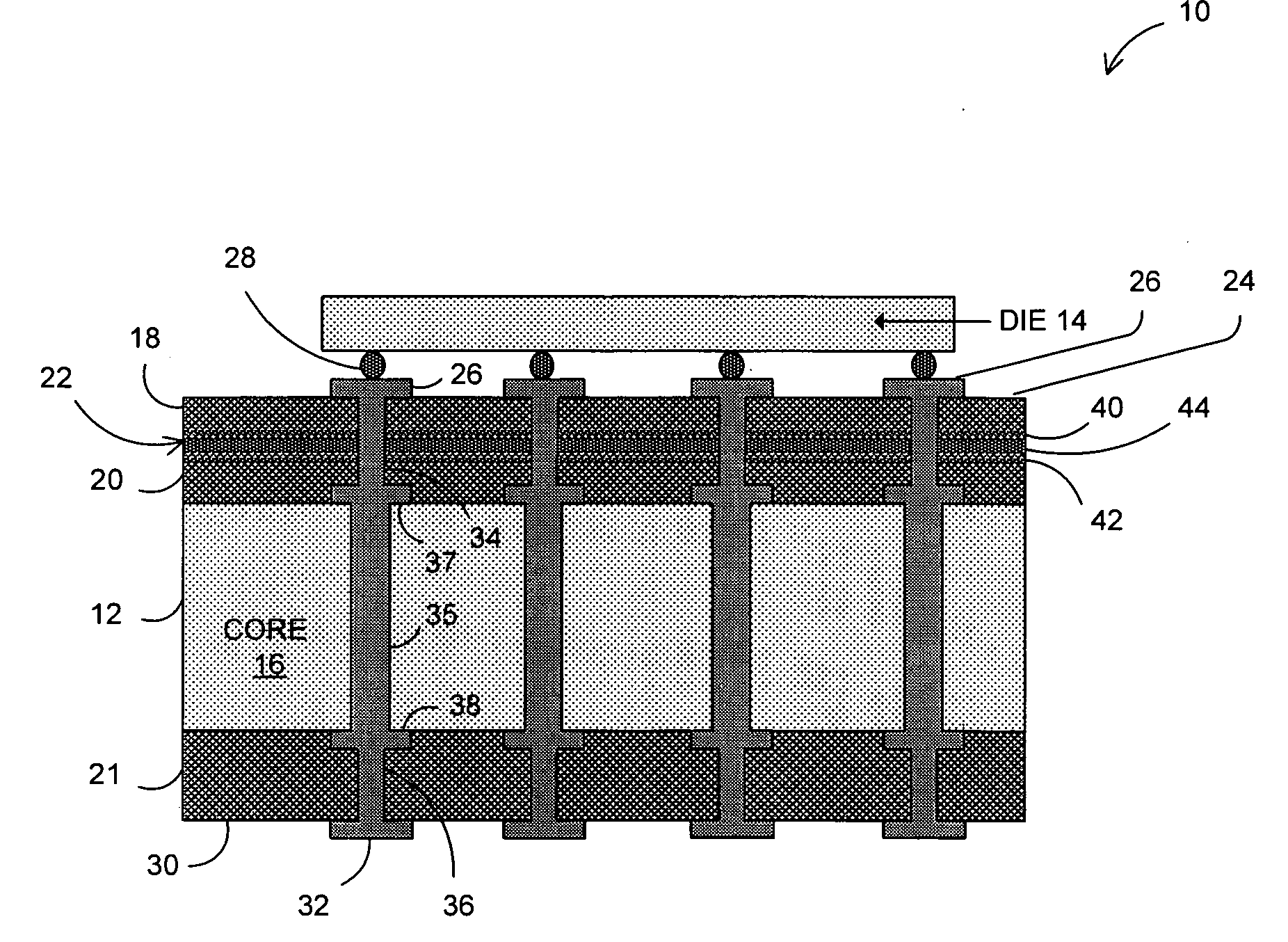
[0018] Referring to FIG. 1, an integrated circuit (IC) package 10 includes a substrate 12 and a die 14 carried by the substrate 12. In one embodiment, the substrate 12 may be a high density interconnect (HDI) substrate. In one embodiment, the substrate 12 may have a core 16, two build-up layers 18 and 20 on one side of the core 16, and a third build-up layer 21 on the other side of the core 16. An integrated thin film capacitor (TFC) 22 may be embedded in the substrate 12 by being sandwiched between the build-up layers 18 and 20 so as to be disposed adjacent to the die 14 to reduce inductance. The buildup layers 18, 20,...


PUM

PropertyMeasurementUnit
Dielectric polarization enthalpyaaaaaaaaaa
Electrical conductoraaaaaaaaaa
Dielectric constantaaaaaaaaaa

Abstract

A method of fabricating an integrated circuit package, comprising prefabricating a film capacitor including forming a first conductive layer, depositing a dielectric layer on the first conductive layer, and depositing a second conductive layer on the dielectric layer; forming a substrate; and laminating the prefabricated film capacitor to the substrate.

Description

BACKGROUND [0001] 1. Technical Field [0002] Embodiments of the present invention are related to the field of electronic devices, and in particular, to integrated circuit packages. [0003] 2. Description of Related Art [0004] An integrated thin film capacitor (TFC) may be embedded in an integrated circuit (IC) package adjacent to a die. The TFC, which may be referred to a decoupling capacitor, stores charge to provide a stable power supply by decoupling the supply from high frequency noise, damping power overshoots when the die is powered up, and damping power droops when the die begins to use power. Inductance between the TFC and the die slows response time of the TFC to voltage changes. By embedding the TFC in close proximity to the die, this inductance may be reduced. [0005] The TFC typically is a multilayer structure with at least one pair of conductive layers (electrodes) coupled between the supply voltage and ground and separated by a dielectric layer or film. Among various diel...

Claims


Application Information

Patent Timeline
IPC IPC(8): B32B37/00H01L21/00
CPCH01L21/4857Y10T156/10H01L2224/16H05K1/112H05K1/162H05K3/16H05K3/382H05K3/4602H05K2201/0317H05K2201/0355H05K2201/09309H05K2201/09509H05K2201/09518H05K2201/096H05K2201/09718H05K2201/10674H01L2924/01019H01L2224/16235H01L23/49822H01L2924/00011H01L2924/00014H01L2224/0401
Inventor MIN, YONGKISALAMA, ISLAM A.
Owner INTEL CORP
Why Eureka
Try Eureka