Organic electro luminescent device and method of manufacturing organic electro luminescent device
a luminescent device and organic technology, applied in the field of electro-optical devices, can solve the problems of degradation of emission efficiency or life, allegedly difficult in general to obtain high patterning accuracy in manufacturing large-screen displays, and the dispersion of chemical species in the light emitting layer, so as to achieve the effect of suppressing the dispersion of chemical species
- Summary
- Abstract
- Description
- Claims
- Application Information
AI Technical Summary
Benefits of technology
Problems solved by technology
Method used
Image

Examples
specific examples
[0121] Some specific examples according to the invention will hereinafter be described.
first specific example
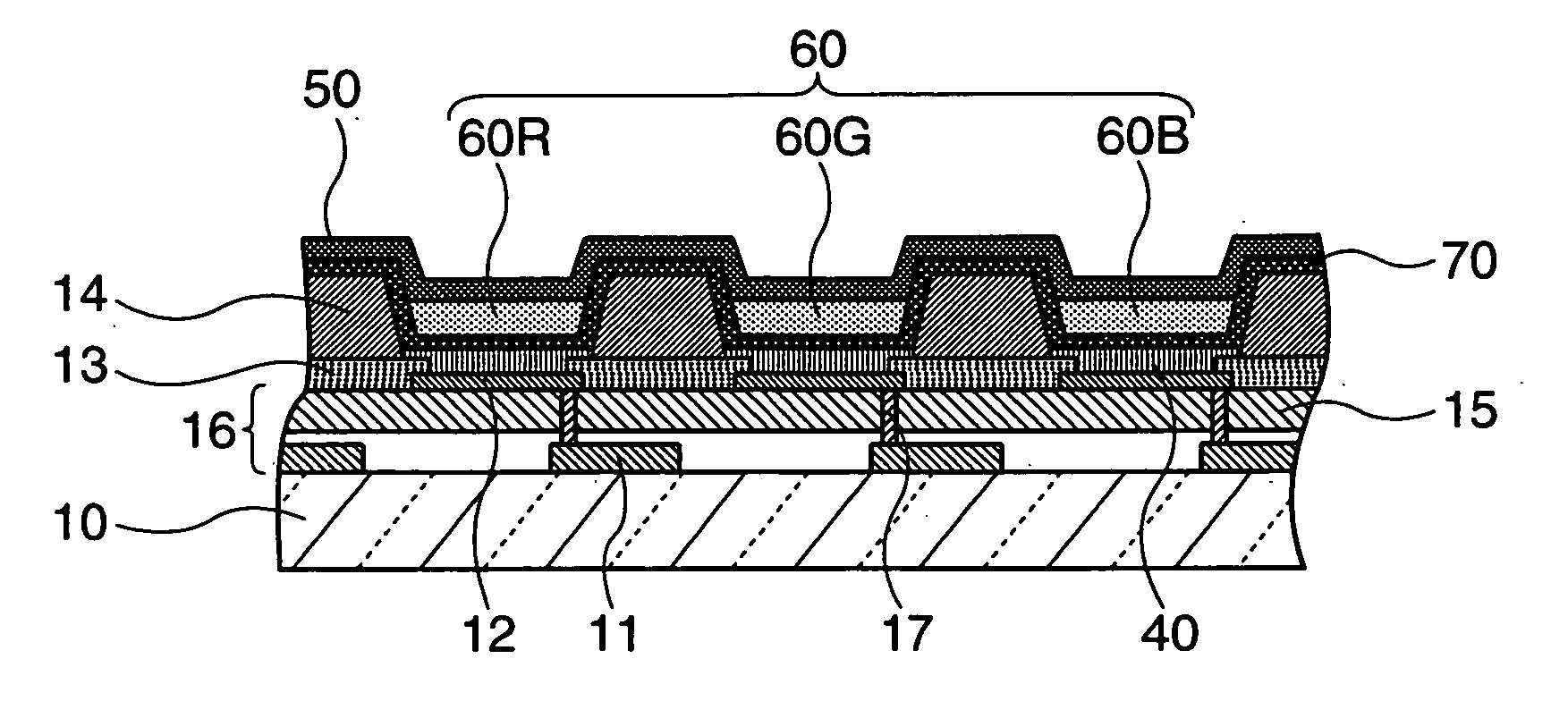
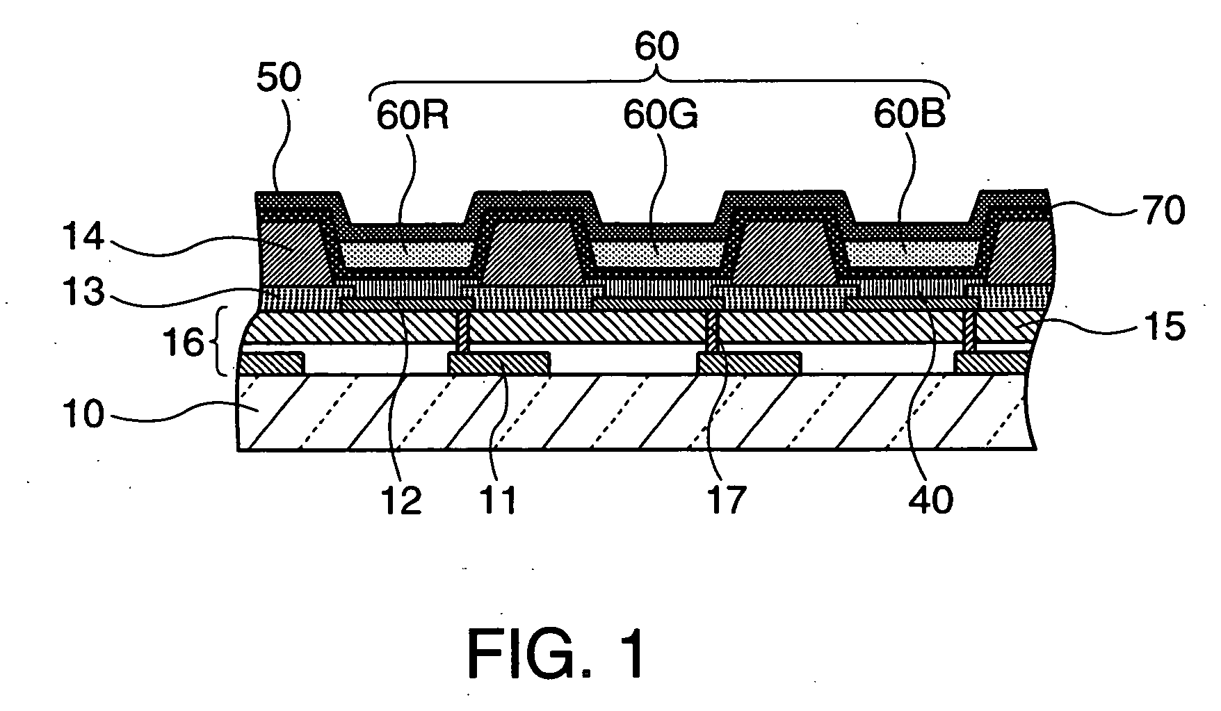
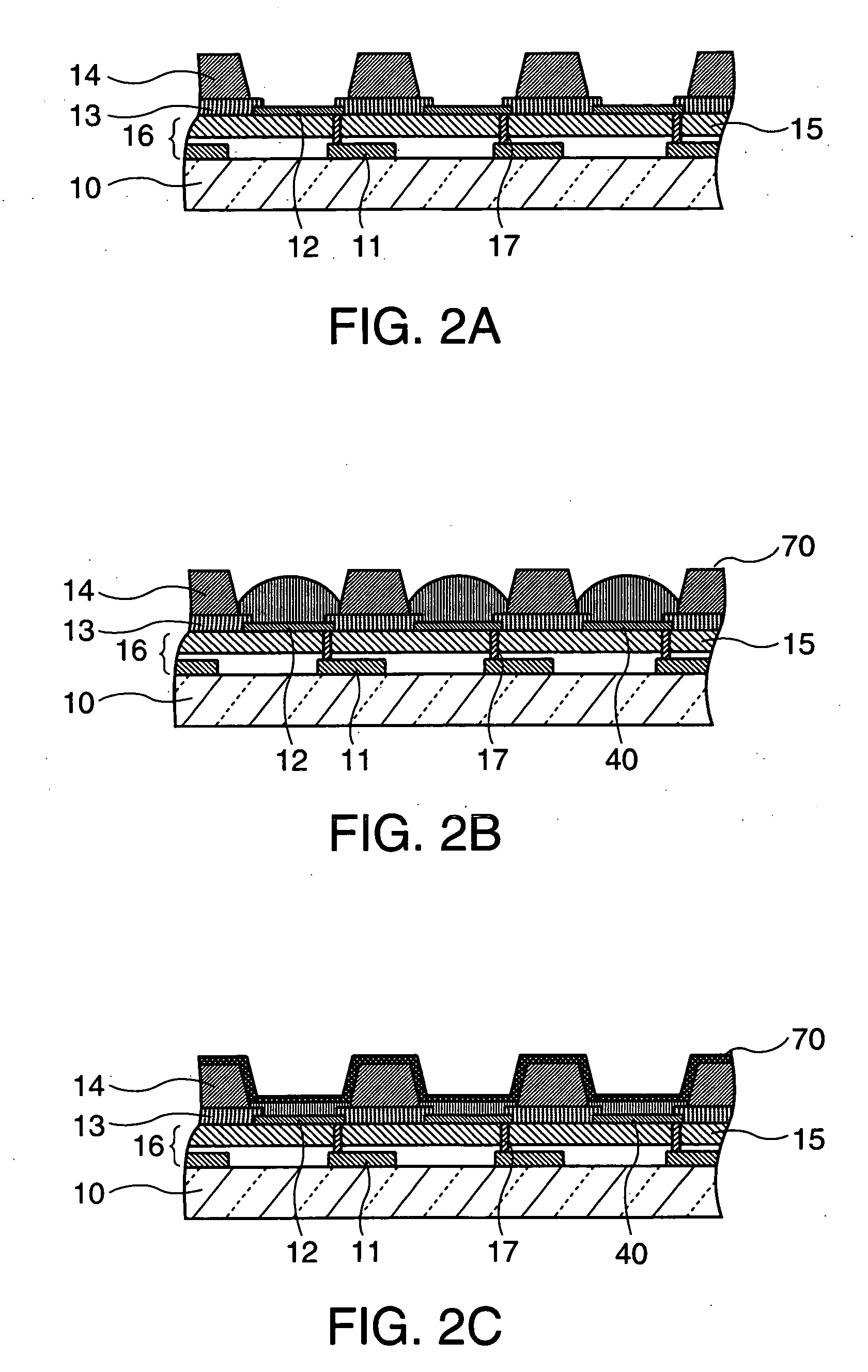
[0122] The pixel electrodes made of ITO were formed on the upper surface of the glass substrate, and then PEDOT / PSS film was formed on the upper surface thereof with a thickness of 600 Å as the hole injection layer using a coating method.
[0123] Further on the upper surface thereof, a polymer film of 30 Å thick was formed as the buffer layer using CHF3 gas in the conditions of the gas flow rate of 50 sccm, the gas pressure of 0.2 Torr, the plasma discharge frequency of 13.56 MHz, and the discharge power of 25 W.
[0124] The light emitting layer was formed on the upper surface thereof using a mixed solution of polydioctylfluorene and F8BT (alternating copolymer of dioctylfluorene and benzothiadiazole).
[0125] On the upper surface of the light emitting layer, 40 Å of LiF film, 50 Å of Ca film, and 2000 Å of Al film composing the cathode were formed by the vacuum evaporation method.
[0126] After then, the whole body was sealed with a sealing substrate.
[0127] In the organic EL device th...
second specific example
[0128] The pixel electrodes made of ITO were formed on the upper surface of the glass substrate, and then PEDOT / PSS film was formed on the upper surface thereof with a thickness of 600 Å as the hole injection layer using a coating method.
[0129] Further on the upper surface thereof, a polymer film of 60 Å thick was formed as the buffer layer using CHF3 gas in the conditions of the gas flow rate of 50 sccm, the gas pressure of 0.2 Torr, the plasma discharge frequency of 13.56 MHz, and the discharge power of 25 W.
[0130] The light emitting layer was formed on the upper surface thereof using a mixed solution of polydioctylfluorene and F8BT (alternating copolymer of dioctylfluorene and benzothiadiazole).
[0131] On the upper surface of the light emitting layer, 40 Å of LiF film, 50 Å of Ca film, and 2000 Å of Al film composing the cathode were formed by the vacuum evaporation method.
[0132] After then, the whole body was sealed with the sealing substrate.
[0133] In the organic EL device ...
PUM
| Property | Measurement | Unit |
|---|---|---|
| Thickness | aaaaa | aaaaa |
Abstract
Description
Claims
Application Information
 - R&D Engineer
- R&D Manager
- IP Professional
- Industry Leading Data Capabilities
- Powerful AI technology
- Patent DNA Extraction
Browse by: Latest US Patents, China's latest patents, Technical Efficacy Thesaurus, Application Domain, Technology Topic.
© 2024 PatSnap. All rights reserved.Legal|Privacy policy|Modern Slavery Act Transparency Statement|Sitemap