Nonvolatile magnetic memory device and photomask

a magnetic memory and non-volatile technology, applied in solid-state devices, nanoinformatics, instruments, etc., can solve the problems of unsatisfactory adoption of such plan-view shapes, inability to realize large-capacity memory, and so on, so as to suppress the dispersions, and reduce the dispersion of the switching magnetic field hswitch

Inactive Publication Date: 2005-12-15
SONY CORP
View PDF2 Cites 21 Cited by
  • Summary
  • Abstract
  • Description
  • Claims
  • Application Information

AI Technical Summary

Benefits of technology

[0186] The plan-view shape of the recording layer in the nonvolatile magnetic memory devices according to the first to eighth embodiments of the present invention is made to be of the Saturn type, whereby the dispersion of the switching magnetic field HSwitch can be reduced, though the reason has not been elucidated. Particularly, even where the magnetoresistance device is damaged due to the dispersion in the lithography step, the processing dispersion in the case of adopting an etching process such as the RIE process and the ion milling process, or etching or an after-treatment (e.g., cleaning treatment in the case of using a chlorine-based gas for etching), the dispersion of the switching magnetic field HSwitch can be largely reduced. As a result, an asteroid characteristic with a large writing operation window, for example, can be obtained, so that it is possible to suppress the dispersions between the nonvolatile magnetic memory devices, and to realize a nonvolatile magnetic memory device which is high in performance and the degree of integration.

Problems solved by technology

Specifically, where the dispersion of the switching magnetic field (HSwitch) is large, the writing margin for the tunnel magnetoresistance devices TMJs is so small that a large-capacity memory cannot be realized.
However, even the adoption of such plan-view shapes is yet unsatisfactory for reducing the dispersion of the switching magnetic field (HSwitch).
In a broader sense, this approach is not satisfactory in terms of the data writing margin for the magnetoresistance devices.

Method used


Image

  • Nonvolatile magnetic memory device and photomask
  • Nonvolatile magnetic memory device and photomask
  • Nonvolatile magnetic memory device and photomask

Examples


example 1

[0211] Example 1 pertains to a nonvolatile magnetic memory device according to the first to fourth embodiments of the present invention. The nonvolatile magnetic memory device in Example 1 including a magnetoresistance device having a recording layer being formed of a ferromagnetic material for storing information by use of variation in resistance depending on the magnetization inversion state thereof, and is specifically a nonvolatile magnetic memory device including a tunnel magnetoresistance device using the TMR effect.

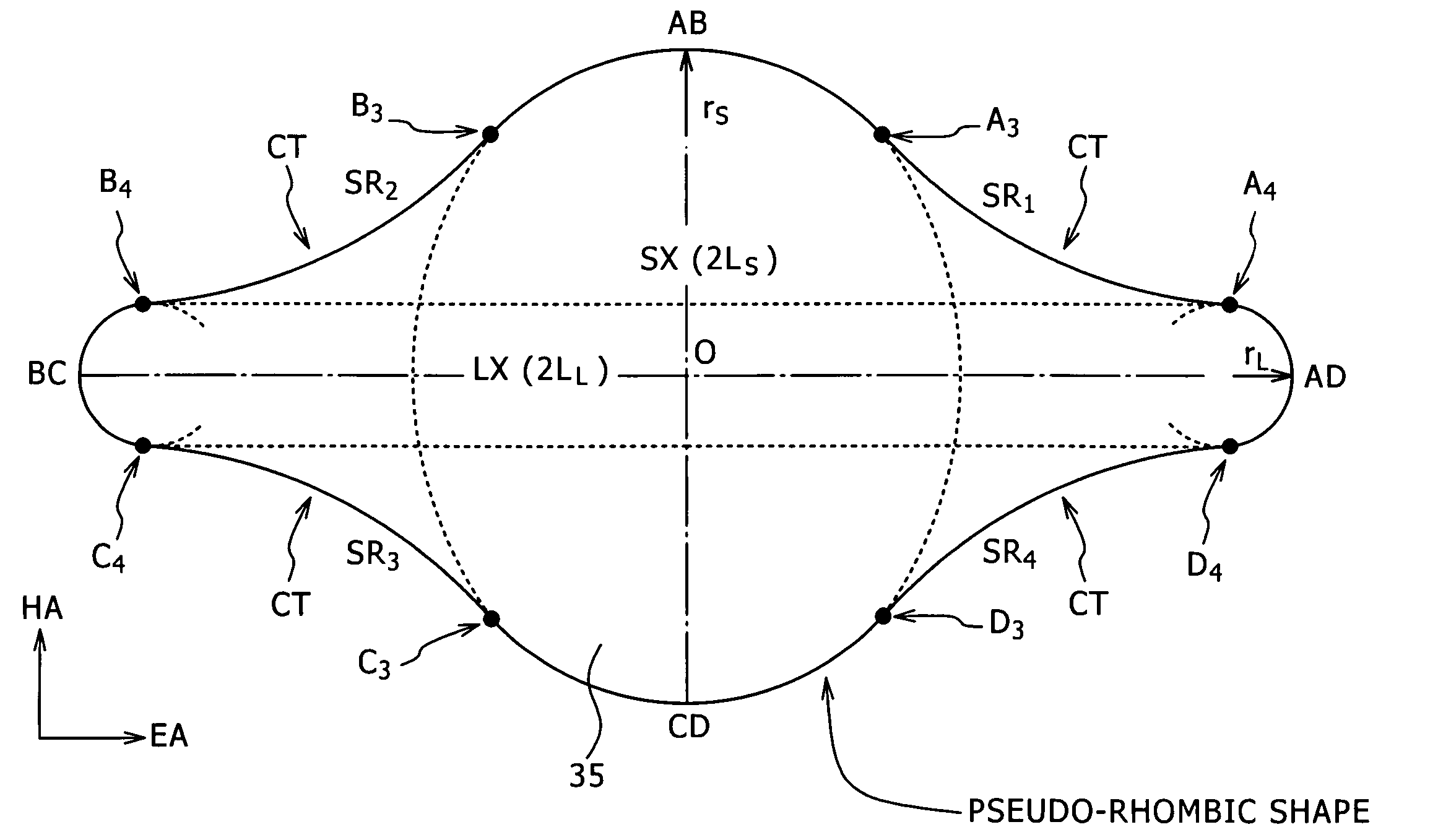
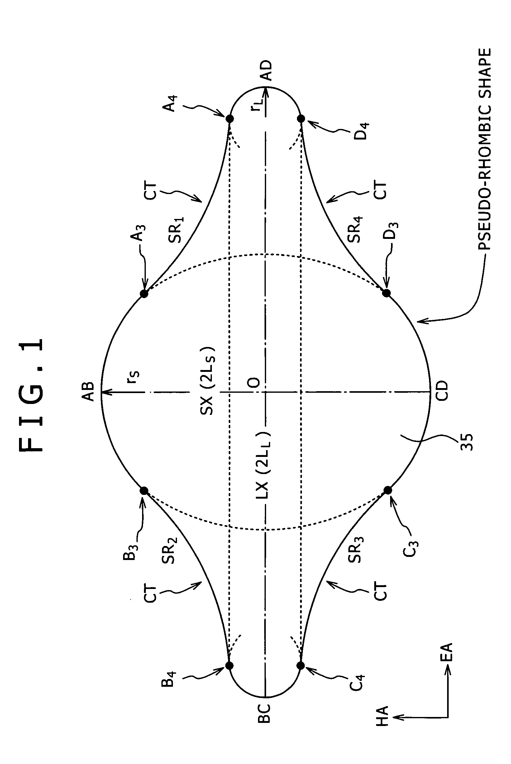
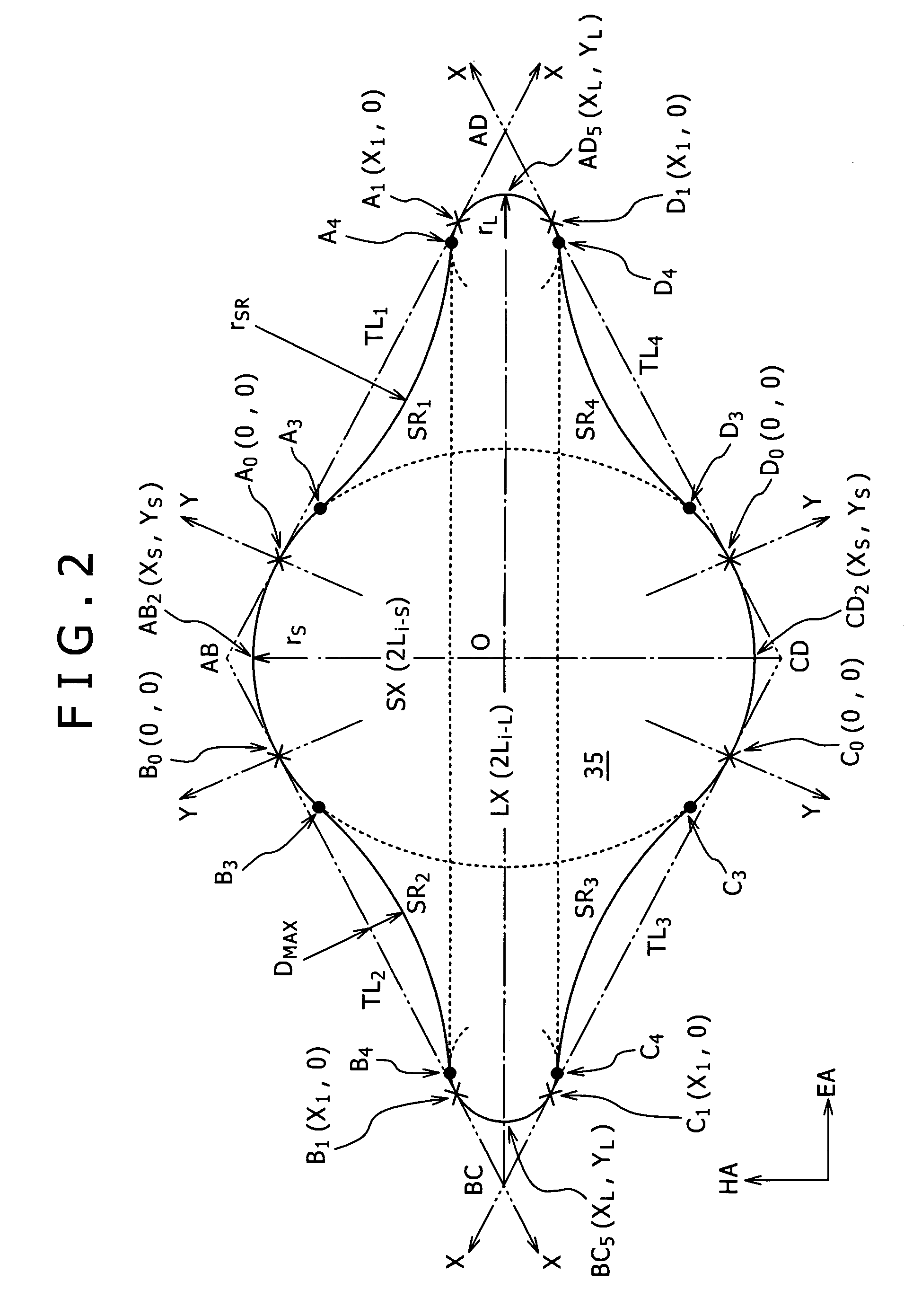
[0212] Here, in the nonvolatile magnetic memory device in Example 1 as the nonvolatile magnetic memory device according to the first embodiment of the present invention, as a schematic plan view of a recording layer 35 is shown in FIG. 1, the plan-view shape (indicated by solid lines) of the recording layer 35 has a pseudo rhombic shape having four sides SRm (where “m” is any of 1, 2, 3, and 4). The sides SRm indicate the portions of the plan-view shape of the rec...

example 2

[0297] Example 2 pertains to the nonvolatile magnetic memory devices according to the fifth to eighth embodiments of the present invention. The nonvolatile magnetic memory deice of Example 2 including a magnetoresistance device having a recording layer formed of a ferromagnetic material for storing information by variation in resistance depending on the magnetization inversion state thereof is also a nonvolatile magnetic memory device including a tunnel magnetoresistance device using the TMR effect, in the same manner as in Example 1. Incidentally, the tunnel magnetoresistance device TMJ and the nonvolatile magnetic memory device in Example 2 also have the same configurations and structures as those of the tunnel magnetoresistance device TMJ and the nonvolatile magnetic memory device in Example 1, except for the difference in the plan-view shape of the recording layer; therefore, the following description will be made only of the plan-view shape of the recording layer.

[0298] Here, ...

example 3

[0332] Example 3 pertains to a photomask according to the one embodiment of the present invention. The photomask in Example 3 is a photomask for use in a lithography step for forming the recording layer 35 described in Example 1 above. Specifically, the recording layer 35 is a recording layer constituting the magnetoresistance device in the nonvolatile magnetic memory device, the recording layer including: [0333] (A) a ferromagnetic material for storing information by use of variation in resistance depending on the magnetization inversion state thereof, [0334] (B) the plan-view shape of the recording layer being a pseudo-rhombic shape, [0335] (C) the four sides SRm constituting the pseudo-rhombic shape each including a smooth curve having a central portion thereof curved toward the center of the pseudo-rhombic shape, [0336] (D) the easy axis (EA) of the recording layer being substantially parallel to the longer axis LX of the pseudo-rhombic shape, [0337] (E) the hard axis (HA) of th...


PUM


Abstract

Disclosed is a nonvolatile magnetic memory device including a magntoresistance device having a recording layer formed of a ferromagnetic material for storing information by use of variation in resistance depending on the magnetization inversion state. The plan-view shape of the recording layer includes a pseudo-rhombic shape having four sides, at least two of the four sides each include a smooth curve having a central portion curved toward the center of the pseudo-rhombic shape. The easy axis of magnetization of the recording layer is substantially parallel to the longer axis of the pseudo-rhombic shape. The hard axis of magnetization of the recording layer is substantially parallel to the shorter axis of the pseudo-rhombic shape. The sides constituting the plan-view shape of the recording layer are smoothly connected to each other.

Description

BACKGROUND OF THE INVENTION [0001] The present invention relates to a nonvolatile magnetic memory device, and a photomask for use in the manufacture of the nonvolatile magnetic memory device. [0002] Attendant on the drastic spread of personal small apparatuses such as communication apparatuses, particularly, the personal digital assistants, various semiconductor devices such as memories and logical circuits constituting the apparatuses are desired to have higher performance, such as higher degree of integration, higher operating speed, lower power consumption, etc. Particularly, nonvolatile memories are considered to be keenly desired in the ubiquitous computing age. Even in the cases of consumption or trouble in the power supply or in the cases of cutoff between a server and a network due to some disorder, the nonvolatile memory makes it possible to preserve and protect important information. In addition, while the recent portable apparatuses are designed to suppress power consumpt...

Claims


Application Information

Patent Timeline
Patent Type & Authority Applications(United States)
IPC IPC(8): G11C11/15G11C11/16G11C11/22H01L27/105H01L21/8246H01L27/22H01L29/82H01L43/08H01L43/12
CPCB82Y10/00H01L43/08H01L27/228G11C11/16H10B61/22H10N50/10G11C11/14
Inventor YAMAGISHI, HAJIME
Owner SONY CORP
Why Eureka
Try Eureka