High-frequency coil device and method of manufacturing the same

a high-frequency coil and coil technology, applied in the direction of transformer/inductance coil/winding/connection, inductance/transformer/magnet manufacturing, etc., can solve the problem of difficulty in the manufacture of conventional high-frequency coil devices, and achieve the effect of high q value and further enhanced q valu

Inactive Publication Date: 2005-09-06
SONY CORP
View PDF3 Cites 20 Cited by
  • Summary
  • Abstract
  • Description
  • Claims
  • Application Information

AI Technical Summary

Benefits of technology

[0020]In the high-frequency coil device according to the first aspect of the present invention, the coil formed of the conductive layer having the predetermined coil pattern is embedded in the surface of the dielectric substrate, and the bottom surface and the side surface of-the coil are covered by, the dielectric substrate, whereby a stable Q value can be achieved, and thus a high-frequency coil device having a stable Q value for GHz band can be implemented. Further, the surface of the high-frequency coil device comprising the coil and the dielectric substrate is set to...

Problems solved by technology

That is, it has been difficult for the conventional high-frequency coil device to manufacture a hig...

Method used


Image

  • High-frequency coil device and method of manufacturing the same
  • High-frequency coil device and method of manufacturing the same
  • High-frequency coil device and method of manufacturing the same

Examples


first embodiment

(First Embodiment)

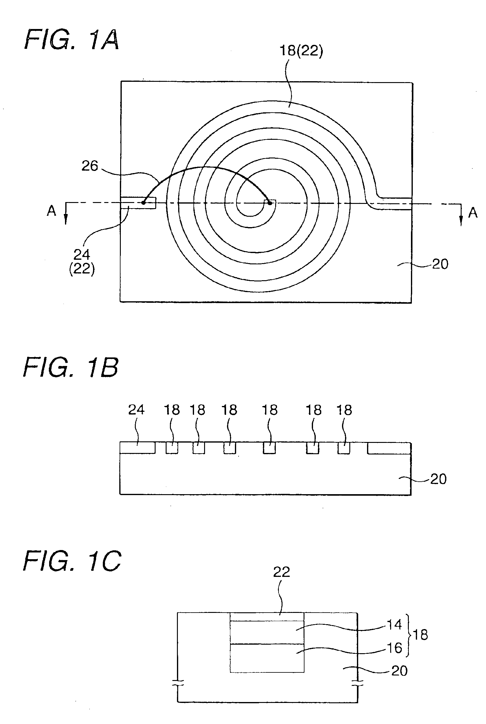
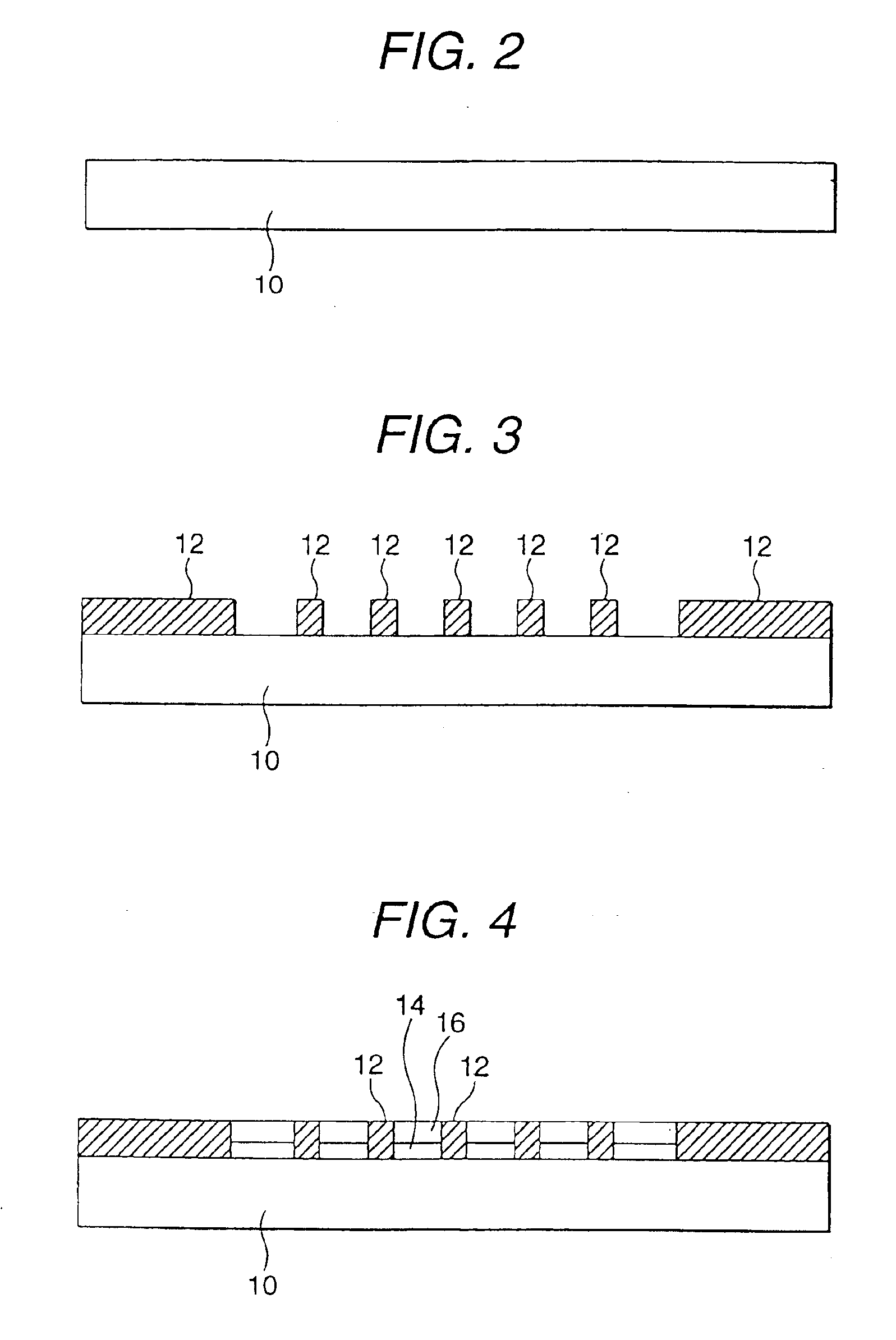
[0041]FIG. 1A is a cross-sectional view showing a high-frequency coil device according to a first embodiment of the present invention, FIG. 1B is a cross-sectional view taken along a line A—A of FIG. 1A, and FIG. 1C is a partially enlarged view of FIG. 1B. FIGS. 2 to 8 are cross-sectional views showing a method of manufacturing a high-frequency coil device according to the embodiment of the present invention.

[0042]In the high-frequency coil device according to this embodiment, a coil 18 having a fine-pitch spiral shape as a predetermined coil pattern is embedded in the surface of a polyimide layer 20 as a dielectric substrate as shown in FIGS. 1A, 1B and 1C. That is, the bottom surface and the side surface of the spirally-shaped coil 18 are coated by the polyimide layer 20.

[0043]The surface of the spirally-shaped coil 18 that is not coated with the polyimide layer 20 is coated with an Au plating layer 22 having a thickness of 0.3 to 5 μm. The surface of the Au plat...

second embodiment

(Second Embodiment)

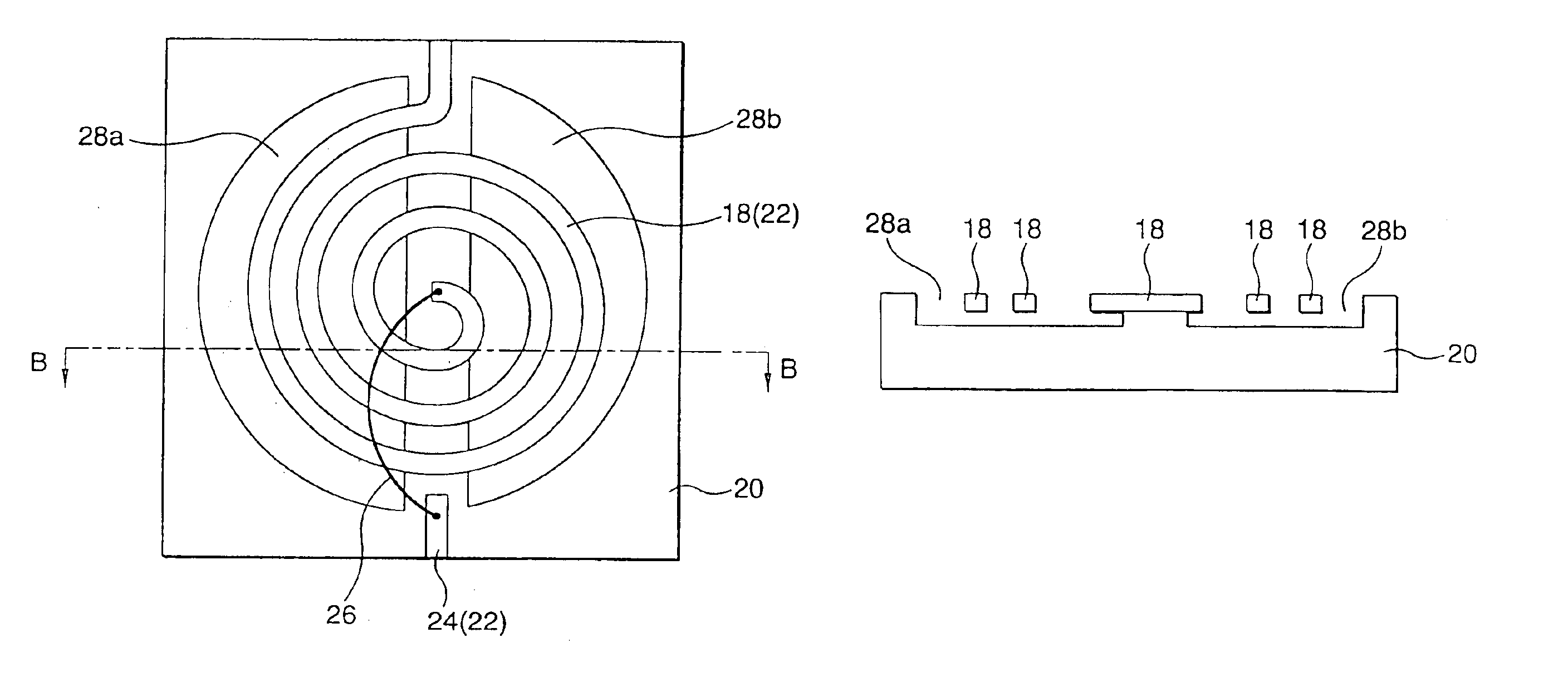
[0066]FIG. 9A is a cross-sectional view showing a high-frequency coil device according to a second embodiment of the present invention, and FIG. 9B is a cross-sectional view taken along a line B—B of FIG. 9A. The same elements as the high-frequency coil device shown in FIG. 1 in the first embodiment are represented by the same reference numerals, and the description of these elements is omitted.

[0067]As shown in FIGS. 9A and 9B, the high-frequency coil device according to this embodiment has substantially the same construction as the high-frequency coil device shown in FIG. 1, however, it is characterized in that two semispherical recesses 28a and 28b are formed on the surface of the polyimide layer 20.

[0068]Therefore, the spirally-shaped fine-pitch coil 18 is embedded in the surface of the polyimide layer 20 as a whole, and the surface of the high-frequency coil device is substantially flat. However, the portions of the spirally-shaped coil 18 which are located w...


PUM

PropertyMeasurementUnit
Dielectric polarization enthalpyaaaaaaaaaa
Electrical inductanceaaaaaaaaaa
Electrical conductoraaaaaaaaaa

Abstract

In a high-frequency coil device having small dispersion in coil inductance and suitable for use in GHz band and a method of manufacturing the high-frequency coil device, a spirally-shaped fine-pitch coil is embedded in the surface of a polyimide layer as a dielectric substrate so that the bottom surface and side surface of the coil is covered by the polyimide layer. The spirally-shaped coil has an Ni—Cu laminate structure in which an Ni plating layer and a Cu plating layer are laminated, and also the side surface thereof is made substantially vertical while the width thereof is uniform with high precision. The surface of the spirally-shaped coil, that is, the surface of the Ni plating layer serving as the upper layer is coated with an Au plating layer.

Description

[0001]This application is a division of Ser. No. 09 / 915,772 filed Jul. 26, 2001, now abandoned.BACKGROUND OF THE INVENTION[0002]1. Field of the Invention[0003]The present invention relates to a high-frequency coil device and a method of manufacturing the same, and particularly to a high-frequency coil device of fine pitch for GHz and a method of manufacturing the same.[0004]2. Description of the Related Art[0005]A conventional high-frequency coil device will be described with reference to FIGS. 10A, 10B and 10C. Here, FIG. 10A is a cross-sectional view showing a conventional high-frequency coil device, FIG. 10B is a cross-sectional view taken along a line C—C of FIG. 10A, and FIG. 10C is a partially enlarged view of FIG. 10B.[0006]As shown in FIGS. 10A, 10B and 10C, a spirally-shaped coil 32a formed of a convex-shaped Cu (copper) layer having a thickness of, for example, 15 to 25 μm is formed on a dielectric substrate 30 formed of polyimide resin having a thickness of, for example, ...

Claims


Application Information

Patent Timeline
IPC IPC(8): H01F17/00H01F41/04H01F5/00
CPCH01F17/0006H01F41/041H01F41/042H01F5/003H01F41/122H01F2017/0046Y10T29/49002Y10T29/4913Y10T29/49073Y10T29/4902Y10T29/49128Y10T29/49139Y10T29/4906H01F5/00
Inventor KUSANO, HIDETOSHI
Owner SONY CORP
Why Eureka
Try Eureka