Formation of deep via airgaps for three dimensional wafer to wafer interconnect

a technology of air gap and deep via, which is applied in the direction of solid-state device manufacturing, electric apparatus, semiconductor/solid-state device manufacturing, etc., can solve the problems of reliability and yield problems, the influence of rc delay, and the inability to spin-on or cvd low-k dielectrics to achieve the effect of wasting valuable surface area

Inactive Publication Date: 2006-10-05
INTERUNIVERSITAIR MICRO ELECTRONICS CENT (IMEC VZW)
View PDF19 Cites 596 Cited by
  • Summary
  • Abstract
  • Description
  • Claims
  • Application Information

AI Technical Summary

Problems solved by technology

For submicron technology, however, RC delay becomes a dominant factor.
While copper and CMP have been integrated smoothly into the IC fabrication process, the same cannot be said for spin-on or CVD low-k dielectrics.
The semiconductor industry has postponed three times (three nodes) the transition to true low-k (k<2.8) ILDs, with reliability and yield problems being the major suspects for the implementation delays.
In the realization of these “through wafer” vias or deep vias there are still a lot of problems to be solved.
A first problem is related to the thermal budget available after etching the deep via through the BEOL, FEOL and subsequent silicon substrate.
A second problem to the creation of said deep vias is related to hardmask selective (etch) processing, which is very difficult to achieve at that stage of the processing.
Said CMP processing is very critical and difficult to perform at that stage of the processing, e.g. damage to the W contact plugs is absolutely to be avoided.

Method used


Image

  • Formation of deep via airgaps for three dimensional wafer to wafer interconnect
  • Formation of deep via airgaps for three dimensional wafer to wafer interconnect
  • Formation of deep via airgaps for three dimensional wafer to wafer interconnect

Examples


Embodiment Construction

[0065] The following description and examples illustrate a preferred embodiment of the present invention in detail. Those of skill in the art will recognize that there are numerous variations and modifications of this invention that are encompassed by its scope. Accordingly, the description of a preferred embodiment should not be deemed to limit the scope of the present invention.

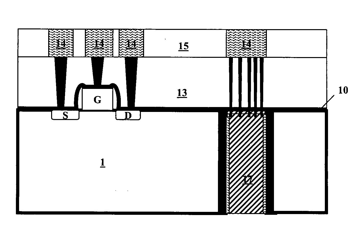
[0066] The term “sacrificial,” as used herein, is a broad term and is used without limitation, as a material or a layer that is deposited temporarily, and that is not supposed to remain, at least totally, in the final device, or a material or layer that is destined to be removed, at least partially, during the process of fabricating a device.

[0067] The term “spacer,” as used herein, is a broad term and is used without limitation, as a material or layer that is deposited o the uncovered parts of the sidewalls of the via that is partially filled with a sacrificial material, in order to narrow the opening of...


PUM


Abstract

A method for forming deep via airgaps in a semiconductor substrate is disclosed comprising the steps of patterning a hole in the substrate, partly fill said hole with a sacrificial material (e.g. poly-Si), forming spacers on the sidewalls of the unfilled part of the hole (e.g. TEOS) to narrow the opening, removing through said narrowed opening the remaining part of the sacrificial material (e.g. by isotropic etching) and finally sealing the opening of the airgap by depositing a conformal layer (TEOS) above the spacers. The method of forming a deep via airgap is used to create wafer to wafer vertical stacking. After completion of conventional FEOL and BEOL processing the backside of the wafer will be thinned such that the deep via airgap is opened and conductive material can be deposited within said (airgap) via opening and a through wafer or deep via filled with conductive material is created.

Description

CROSS REFERENCE TO RELATED APPLICATION [0001] This application claims the benefit of U.S. Provisional Application No. 60 / 637,288, filed Dec. 17, 2004, which is incorporated by reference herein in its entirety, and is hereby made a portion of this specificationFIELD OF THE INVENTION [0002] The present invention is related to the field of forming deep vias filled with a gas (air) in a semiconductor substrate, also referred to as deep via airgaps. Said deep via airgaps are used to create through wafer vias filled with conductive material for three dimensional (3D) wafer to wafer interconnect structures also referred to as vertically stacking of wafers or three dimensional semiconductor integrated circuit devices. BACKGROUND OF THE INVENTION [0003] For decades, semiconductor manufacturers have been shrinking transistor size in ICs to achieve the yearly increases in speed and performance described by Moore's Law—chip performance will double every ˜18 months. Moore's Law exists only becau...

Claims


Application Information

Patent Timeline
Patent Type & Authority Applications(United States)
IPC IPC(8): H01L21/4763
CPCH01L21/762H01L21/76289H01L21/764H01L21/76898H01L23/481H01L25/0657H01L25/50H01L2924/0002H01L2221/1094H01L2225/06513H01L2225/06541H01L2924/00
Inventor VANHAELEMEERSCH, SERGEKUNNEN, EDDYCARBONELL, LAURE ELISA
Owner INTERUNIVERSITAIR MICRO ELECTRONICS CENT (IMEC VZW)
Why Eureka
Try Eureka