Plating buss and a method of use thereof

a technology of plating bus and dicing saw, which is applied in the direction of printed circuit manufacturing, printed circuit aspects, conductive pattern reinforcement, etc., can solve the problems of indexing errors, blade and/or stage drift of dicing saw, and no useful function of plating bus, so as to reduce short circuit problems, increase the yield of boards, and improve the sawn edge of each finished pcb.

Inactive Publication Date: 2006-10-12
MICRON TECH INC
View PDF15 Cites 2 Cited by
  • Summary
  • Abstract
  • Description
  • Claims
  • Application Information

AI Technical Summary

Benefits of technology

[0010] In view of the foregoing considerations, the present invention is directed to an improved plating buss, wherein the plating buss connecting traces of adjacent printed circuit board (PCB) in a substrate panel are provided in a serpentine design. The serpentine plating buss widens the PCB singulation process window, thereby minimizing short circuit problems often seen in PCB singulation due to indexing errors resulting from occasional manufacturing variations and alignment problems. Accordingly, the serpentine plating buss of the present invention increases board yield. Another benefit of the serpentine plating buss is that the sawn edge of each finished PCB may be improved due to the fact that no longer must PCB singulation be directly on top of the entire plating buss in order to disconnect joined conductive traces.

Problems solved by technology

However, a plating buss serves no useful function after the electroplating process.
However, over time, the blade and / or stage of the dicing saw may experience drift due to indexing errors of its drive motor and associated gearing.
Additionally, variations in the PCB manufacturing process effecting PCB sizes and street locations, and variations in blade width due to uneven heating and wear can also result in indexing errors.

Method used


Image

  • Plating buss and a method of use thereof
  • Plating buss and a method of use thereof
  • Plating buss and a method of use thereof

Examples


Embodiment Construction

[0023]FIGS. 3a-3d provides a step-by-step explanation of a printed circuit manufacturing technique used to form a plating buss according to the present invention. In conjunction with this explanation, FIGS. 4 and 5 each present a top elevation of a substrate panel having a plurality of adjacent printed circuit boards (PCBs) thereon and bearing conductive traces connected by a plating buss according to the present invention. FIGS. 6a-6c are illustrations of various serpentine plating buss embodiments according to the present invention.

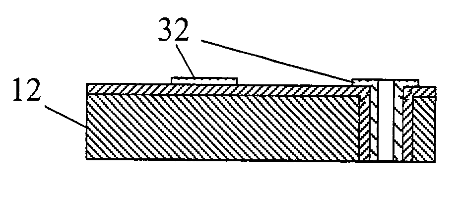
[0024] With reference to FIG. 3a, manufacturing of a plurality of PCBs 10 begins similar to most other commonly used additive techniques. Namely, an unclad laminated substrate panel 12 used for forming the plurality of PCBs 10 is first provided. The panel 12 is normally made of a nonconductive material, such as phenolic, glass-impregnated epoxy, polymide, FR4, FR5 or the like. The panel 12 is then drilled in accordance with a predetermined pattern, suc...


PUM

PropertyMeasurementUnit
non-conductiveaaaaaaaaaa
conductiveaaaaaaaaaa
electrical conductivityaaaaaaaaaa

Abstract

The present invention relates generally to a plating buss design and method for minimizing short circuit problems in PCB panel singulation. More particularly, the invention encompasses a serpentine plating buss which increases the PCB singulation process window thereby minimizing short circuit problems due to indexing errors caused by occasional manufacturing and equipment alignment problems. The serpentine plating buss design therefore increases board yield.

Description

CROSS REFERENCE TO RELATED APPLICATION [0001] This application is a divisional of U.S. patent application Ser. No. 10 / 861,847, filed Jun. 4, 2004.BACKGROUND OF THE INVENTION [0002] The present invention relates generally to the field of printed circuit fabrication, and more particularly to an improved plating buss on a substrate such as for example a printed circuit board (PCB), which addresses manufacturing variations and alignment problems associated with PCB singulation for improved board yield. [0003] Basically, a printed circuit board consists of a sheet of rigid insulating substrate such as phenolic, glass impregnated epoxy or the like, having a pre-defined pattern of thin metallic—usually copper—foil conductive paths (so-called “traces”) appearing on one or both sides of the substrate. These traces collectively define all the electrical interconnections among all the components and are routed between appropriate locations on the board. [0004] Electrolytic plating is one metho...

Claims


Application Information

Patent Timeline
Patent Type & Authority Applications(United States)
IPC IPC(8): H05K1/11H05K3/00H05K3/24
CPCH05K3/0052H05K3/242H05K2201/09263Y10T29/49165Y10T29/49155Y10T29/49126Y10T29/49117
Inventor JOHNSON, MARK S.
Owner MICRON TECH INC
Why Eureka
Try Eureka