Liquid crystal display device and method of fabricating the same

a display device and liquid crystal technology, applied in non-linear optics, instruments, optics, etc., can solve the problems of difficult to present a stable image, increase the number of processes, poor contrast ratio, etc., to enhance the aperture ratio of multi-domains, and reduce the number of fabrication process steps

Active Publication Date: 2006-10-12
LG DISPLAY CO LTD
View PDF5 Cites 11 Cited by
  • Summary
  • Abstract
  • Description
  • Claims
  • Application Information

AI Technical Summary

Benefits of technology

[0015] An object of the present invention is to reduce the number of fabrication process steps for forming multi-domains in each of the pixels of a liquid crystal display device. and enhancing an aperture ratio by structuring the LCD.
[0016] Another object of the present invention is to enhance an aperture ratio of multi-domains in each of the pixels of a liquid crystal display device.

Problems solved by technology

However, since light is not completely cut off during the off-state in a TN mode LCD, a contrast ratio is poor.
Accordingly, it is difficult to present a stable image because halftone brightness varies as the viewing angle is varied.
Therefore, there is a drawback in that the number of the process inevitably increases the implementation of multi-domains in each pixel region.

Method used


Image

  • Liquid crystal display device and method of fabricating the same
  • Liquid crystal display device and method of fabricating the same
  • Liquid crystal display device and method of fabricating the same

Examples


Embodiment Construction

[0030] Reference will now be made in detail to the preferred embodiments of the present invention, examples of which are illustrated in the accompanying drawings. Wherever possible, the same reference numbers will be used throughout the drawings to refer to the same or like parts.

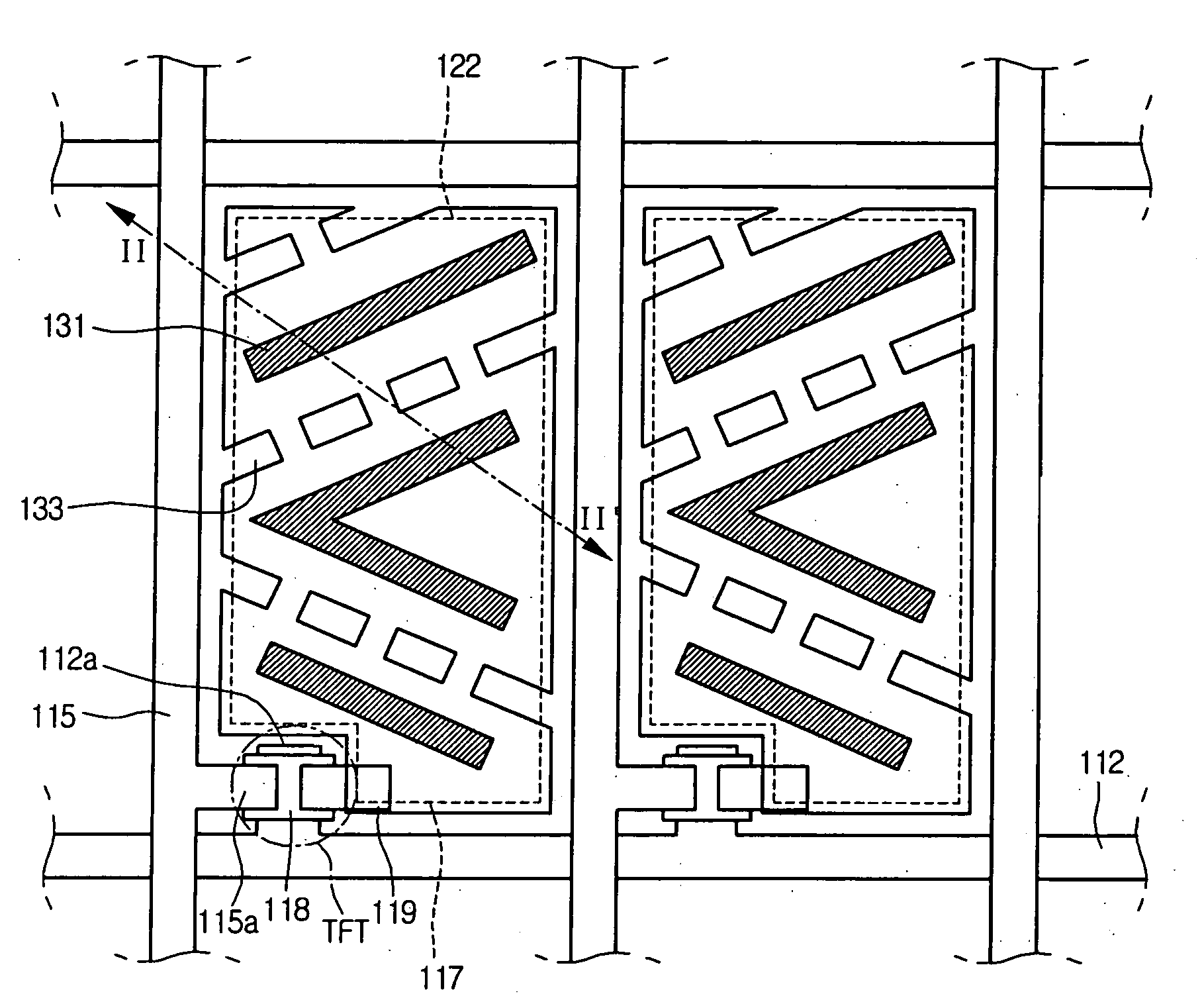
[0031]FIG. 3 is a plan view of an LCD according to an embodiment of the present invention, and FIG. 4 is a cross-sectional view taken along the line II-II′ of FIG. 3. Referring to FIGS. 3 and 4, the MVA mode LCD in an embodiment of the present invention includes an upper substrate 121, a lower substrate 111 and a layer of liquid crystal molecules interposed therebetween. The lower substrate 111 includes a gate line 112 and a data line 15, which are respectively arranged in a row direction and a column direction, and cross each other to define a pixel region. A pixel electrode 117 is formed in the pixel region. A thin film transistor is (TFT) formed adjacent to the crossing of the gate line 112 and the data...


PUM

PropertyMeasurementUnit
electric fieldaaaaaaaaaa
electric field distortionaaaaaaaaaa
voltageaaaaaaaaaa

Abstract

A liquid crystal display device includes: a first substrate and a second substrate; a gate line and a data line on the first substrate that cross each other to define a pixel region; a pixel electrode in the pixel region; a thin film transistor at the crossing of the gate and data lines, and connected to the pixel electrode; at least one first electric field distortion unit in the pixel electrode to control a liquid crystal director by electric field distortion; a second electric field distortion unit between the pixel electrode and the first substrate; and a layer of liquid crystal molecules between the first and second substrates

Description

[0001] The present invention claims the benefit of Korean Patent Application No. 029982 / 2005 filed in Korea on Apr. 11, 2005, which is hereby incorporated by reference in its entirety. BACKGROUND OF THE INVENTION [0002] 1. Field of the Invention [0003] The present invention relates to a display device, and more particularly, to a liquid crystal display device. Although the present invention is suitable for a wide scope of applications, it is particularly suitable for forming multi-domains in each of the pixels of a liquid crystal display device. [0004] 2. Description of the Related Art [0005] One of the types of liquid crystal displays (LCDs) typically used in most recent years is a twisted nematic (TN) mode LCD. The structure of a TN mode LCD includes two substrates on which respective electrodes are formed and a layer of liquid crystal molecules between the two substrates. The liquid crystal molecules within the layer have a long shape oriented parallel to each of the two substrat...

Claims


Application Information

Patent Timeline
Patent Type & Authority Applications(United States)
IPC IPC(8): G02F1/1337
CPCG02F1/133707G02F1/1393G02F1/133753G02F1/1343
Inventor AHN, JI YOUNGSON, HYEON HO
Owner LG DISPLAY CO LTD
Why Eureka
Try Eureka