Multiple-wavelength light emitting diode and its light emitting chip structure

a light emitting diode and multi-wavelength technology, applied in the direction of basic electric elements, electrical appliances, semiconductor devices, etc., can solve the problems of reducing the overall difficult to control the composition of the bonding material, and inability to precisely control the quality of light colors for the overall so as to achieve the effect of enhancing the brightness performance of the light emitting diod

Inactive Publication Date: 2006-10-19
TAIWAN OASIS TECH CO LTD
View PDF5 Cites 3 Cited by
  • Summary
  • Abstract
  • Description
  • Claims
  • Application Information

AI Technical Summary

Benefits of technology

[0007] It is a primary objective of the present invention to provide a multiple-wavelength light emitting diode comprising a fluorescent layer with a predetermined wavelength disposed at the bottom of the light emitting diode, such that a light emitting chip can be fixed onto a carrier and connected in parallel with the circuit of the light emitting chip. The light emitting chip is packaged by a package material to constitute a light emitting diode that combines the light source of the light emitting chip with the wavelength of the fluorescent layer, so as to produces the desired light color. Since the fluorescent layer is fixed onto the bottom of the light emitting diode in advance, therefore the coating area and the coating quantity can be controlled effectively and the quality of light color produced by the fluorescent layer can be controlled precisely. Even more, a reflective material installed at the lowest fluorescent layer under the light emitting chip can effectively enhance the brightness performance of the light emitting diode.

Problems solved by technology

However, such arrangement implants some regions at the bottom of the light emitting chip 20 into the bonding material 40, and thus reducing the overall brightness performance of the light emitting diode.
Furthermore, it is not easy to control the composition of the bonding material 40, the coating area and the coating quantity, although the bonding material 40 is mixed with a fluorescent material to combine the light source of the light emitting chip with the wavelength of the fluorescent material to produce expected light colors, and thus it is unable to precisely control the quality of light colors for the overall performance of the light emitting diode.

Method used


Image

  • Multiple-wavelength light emitting diode and its light emitting chip structure
  • Multiple-wavelength light emitting diode and its light emitting chip structure
  • Multiple-wavelength light emitting diode and its light emitting chip structure

Examples


Embodiment Construction

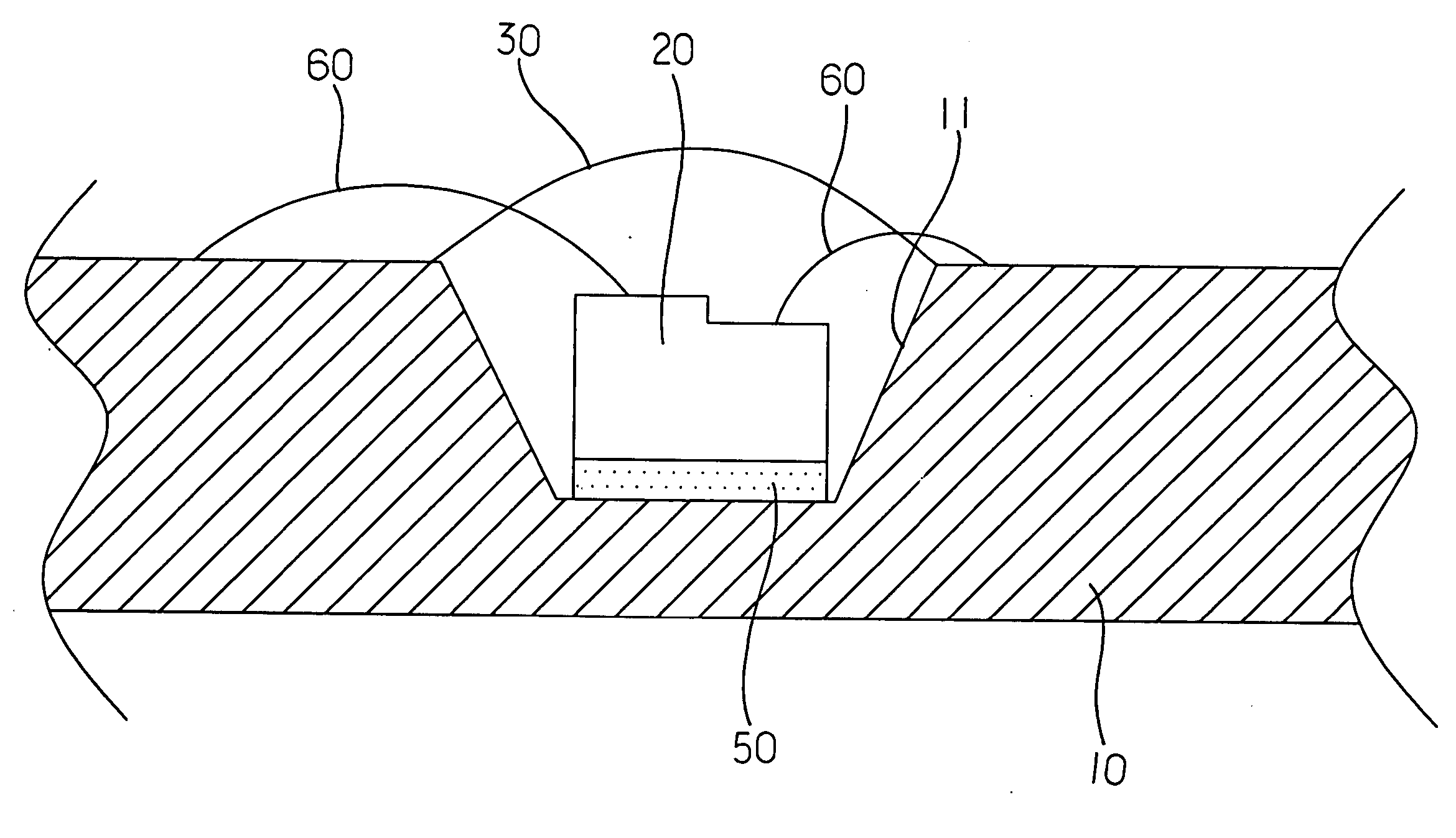
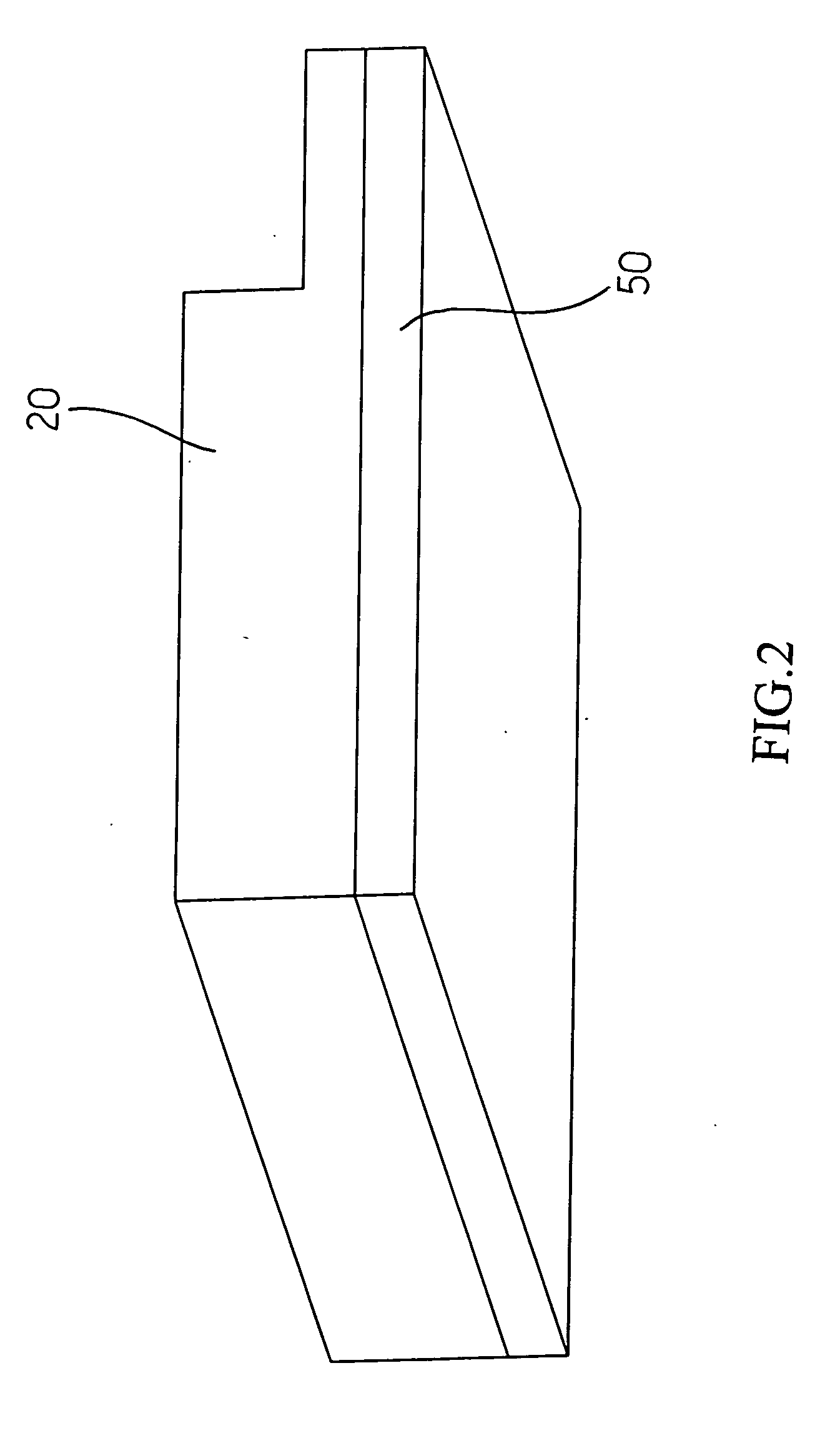
[0016] The multiple-wavelength light emitting diode in accordance with the present invention provides a light emitting diode and its light emitting chip structure capable of producing a correct light color and effectively enhancing the brightness performance. In FIG. 2, the light emitting chip 20 includes a fluorescent layer 50 having a predetermined wavelength and disposed at the bottom of the light emitting chip 20, and the fluorescent layer 50 could be made of a single fluorescent power or made by mixing two or more fluorescent powders according to a predetermined proportion. In FIG. 3, the light emitting chip 20 is fixed into a predetermined space (or a carrier having a similar function) on the substrate 10 and the circuit of the light emitting chip 20 is connected in parallel by a gold wire 60. The light emitting chip 20 is packaged by a package material 30, so that the light source of the light emitting chip 20 can be combined with the wavelength of the fluorescent layer 50, s...


PUM


Abstract

The present invention discloses a multiple-wavelength light emitting diode that includes a fluorescent layer with a predetermined wavelength disposed at the bottom of the light emitting diode, such that a light emitting chip can be fixed onto a carrier and connected in parallel with the circuit of the light emitting chip by a gold wire. The light emitting chip is packaged by a package material to constitute a light emitting diode capable of combining the light source of the light emitting chip with the wavelength of the fluorescent layer, so as to produces the desired light color.

Description

BACKGROUND OF THE INVENTION [0001] 1. Field of the Invention [0002] The present invention relates to a color light performance technology of a light emitting diode, and more particularly to a light emitting diode and its light emitting chip structure capable of producing correct light colors and enhance brightness performance effectively. [0003] 2. Description of the Related Art [0004] In general, a basic structure of a light emitting diode includes a related package material to package a light emitting chip, and a gold wire used to electrically connect the light emitting chip with related circuits. The light emitting chip produces a light source after the light emitting chip is electrically connected. The light source is projected outward from the package material and further combined with the wavelength of a fluorescent material in the package material to produce a desired light color. [0005] Referring to FIG. 1, the present common traditional light emitting diode structure direct...

Claims


Application Information

Patent Timeline
Patent Type & Authority Applications(United States)
IPC IPC(8): H01L31/12
CPCH01L33/501H01L33/505H01L33/60H01L24/32H01L2224/48091H01L2224/49107H01L2224/45144H01L2224/73265H01L2924/00H01L2924/12041H01L2224/8592H01L2224/83385H01L2224/32225H01L2924/15153H01L2924/00014
Inventor LEE, MING-SHUNSUNG, PING-RUHO, CHANG-WEI
Owner TAIWAN OASIS TECH CO LTD
Why Eureka
Try Eureka