Method and structure for ion implantation by ion scattering

a technology of ion scattering and ion implantation, which is applied in the direction of semiconductor devices, electrical apparatus, transistors, etc., can solve the problems of affecting the size of the device, and unwanted doping can introduce negative characteristics to the completed device,

Inactive Publication Date: 2006-10-19
GLOBALFOUNDRIES INC
View PDF17 Cites 13 Cited by
  • Summary
  • Abstract
  • Description
  • Claims
  • Application Information

AI Technical Summary

Problems solved by technology

As semiconductor devices have been reduced in size, certain effects which were inconsequential at larger device sizes become problematic at smaller device sizes.
In situations where the u

Method used


Image

  • Method and structure for ion implantation by ion scattering
  • Method and structure for ion implantation by ion scattering
  • Method and structure for ion implantation by ion scattering

Examples


Embodiment Construction

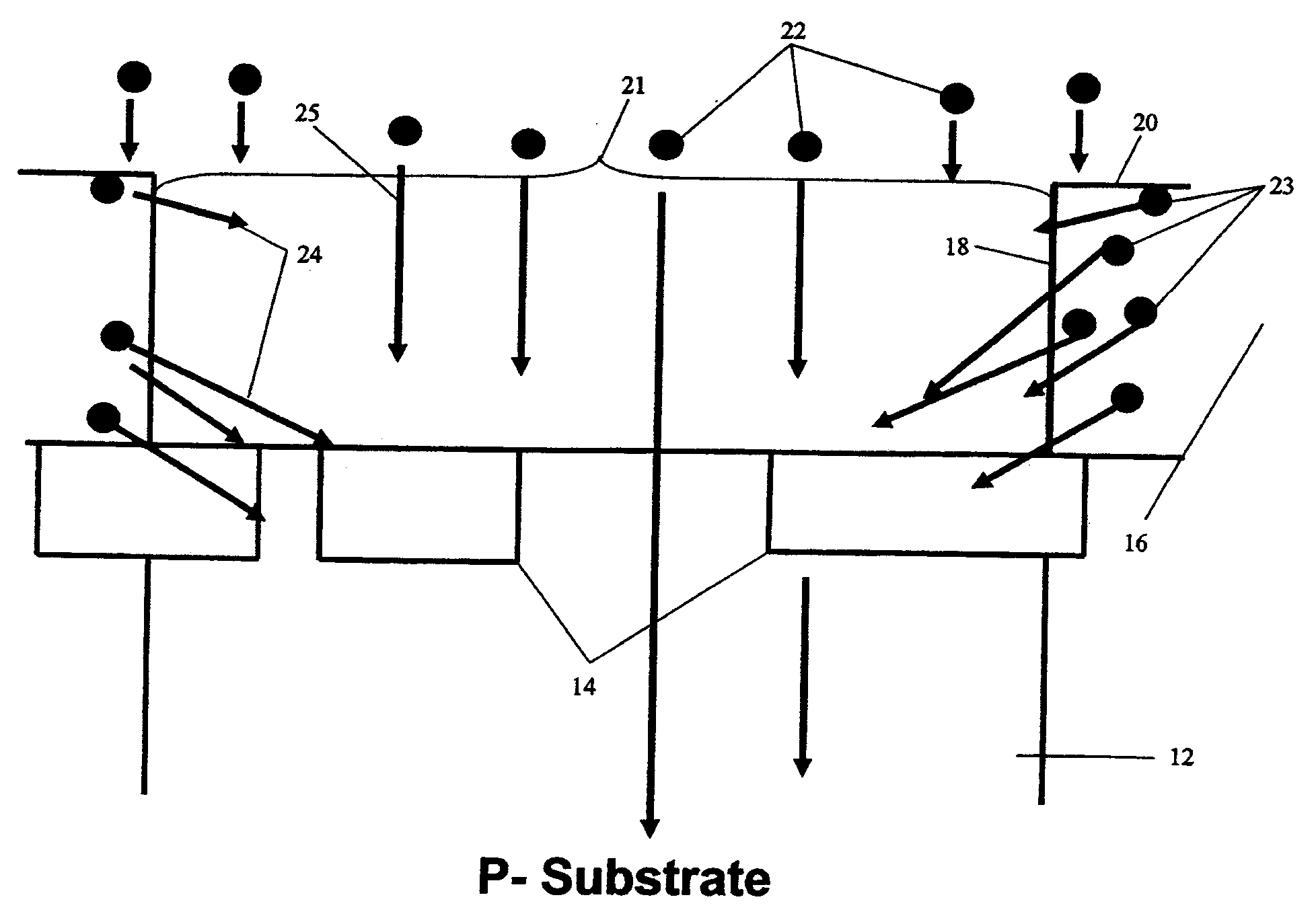
[0016] The invention produces semiconductor devices having different break down voltages in a single ion implantation process. Thus, the invention can provide semiconductor devices and circuits incorporating the semiconductor devices where one particular device has a lower breakdown voltage than another particular device formed during a single doping step. Thus, the invention allows semiconductor devices to be fabricated with different breakdown voltages in one ion implantation operation. This is accomplished by forming a bi-level implantation using a scatter implantation process. For example, the scatter implantation process of the invention can rely on the edge of the mask to scatter ions into an adjacent unmasked substrate where the scattered ions have a lower energy than non-scattered ions. The low energy ions will be deposited near the surface of the substrate while the higher energy non-scattered ions will be deposited at a greater depth in the substrate.

[0017] Referring to F...


PUM


Abstract

A scatter-implant process and device is provided where a bi-level doping pattern is achieved in a single doping step. Additionally, devices having different breakdown voltages can be produced in a single implant process. The scatter-implant is fabricated by scattering implant ions off the edge of a mask, thereby reducing the ion energy causing the ions to doping shallower regions than the non-scattered ions which dope a lower region. By adjusting various parameters of the doping process such as, for example, ion type, ion energy, mask type and geometry, in a position of scattering edge relative to other structure of the device, the scatter-implant can be tuned to achieve certain properties of the semiconductor device. Additionally, circuits can be made using the scatter-implant process where pre-selected portion of the circuit incorporate the scatter-implant region and other portions of the circuit do not rely on the scatter region.

Description

FIELD OF THE INVENTION [0001] The invention relates to doping a substrate, and more particularly to doping a substrate by passing the dopant through a scattering layer. BACKGROUND DESCRIPTION [0002] As semiconductor devices have been reduced in size, certain effects which were inconsequential at larger device sizes become problematic at smaller device sizes. For example, where regions in a particular device are formed by implanting ions in a doping process, the ions are typically deposited from directly above the region to be implanted. Additionally, the ions typically will travel a certain distance through a material before losing energy and coming to a stop thereby forming a doped region. As an example, during the formation of an implanted sub-collector, ions are deposited from directly above the region to form the implanted sub-collector. In this example, the ions will travel through a predetermined amount of material before lodging in a region in the material to form the implant...

Claims


Application Information

Patent Timeline
IPC IPC(8): H01L21/22H01L21/38
CPCH01L21/266H01L29/7378H01L29/66242H01L27/0259
Inventor LANZEROTTI, LOUIS D.SHERIDAN, DAVID C.VOLDMAN, STEVEN H.
Owner GLOBALFOUNDRIES INC
Why Eureka
Try Eureka