Plasma display panel

a technology of display panel and plasma, which is applied in the direction of electrodes, lighting and heating apparatus, furniture, etc., can solve the problems of reducing the brightness of the panel and reducing the luminous efficiency

Inactive Publication Date: 2006-10-26
SAMSUNG SDI CO LTD
View PDF17 Cites 10 Cited by
  • Summary
  • Abstract
  • Description
  • Claims
  • Application Information

AI Technical Summary

Benefits of technology

[0008] It is therefore an object of the present invention

Problems solved by technology

Therefore, luminous efficiency and

Method used


Image

  • Plasma display panel
  • Plasma display panel
  • Plasma display panel

Examples


first embodiment

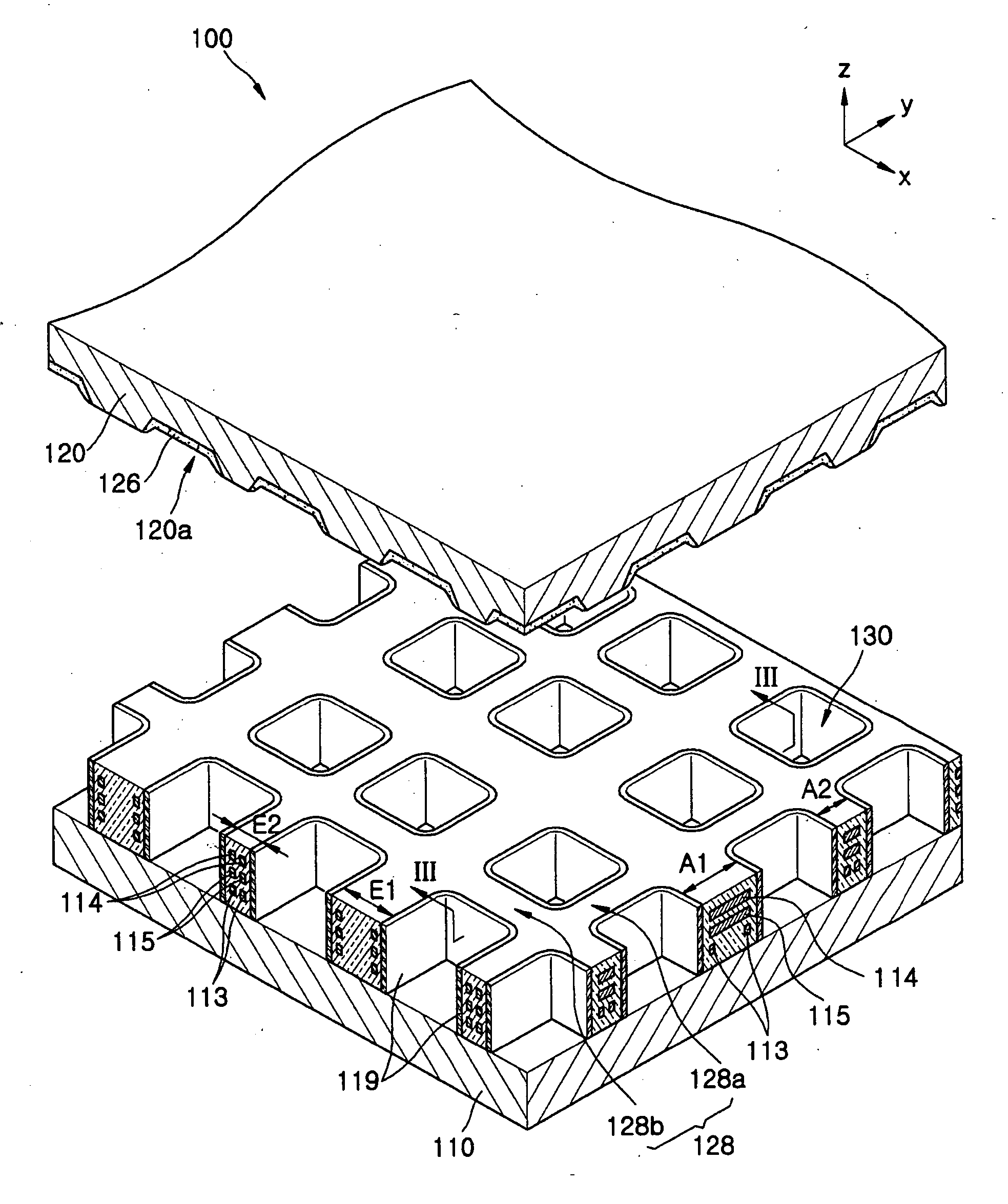
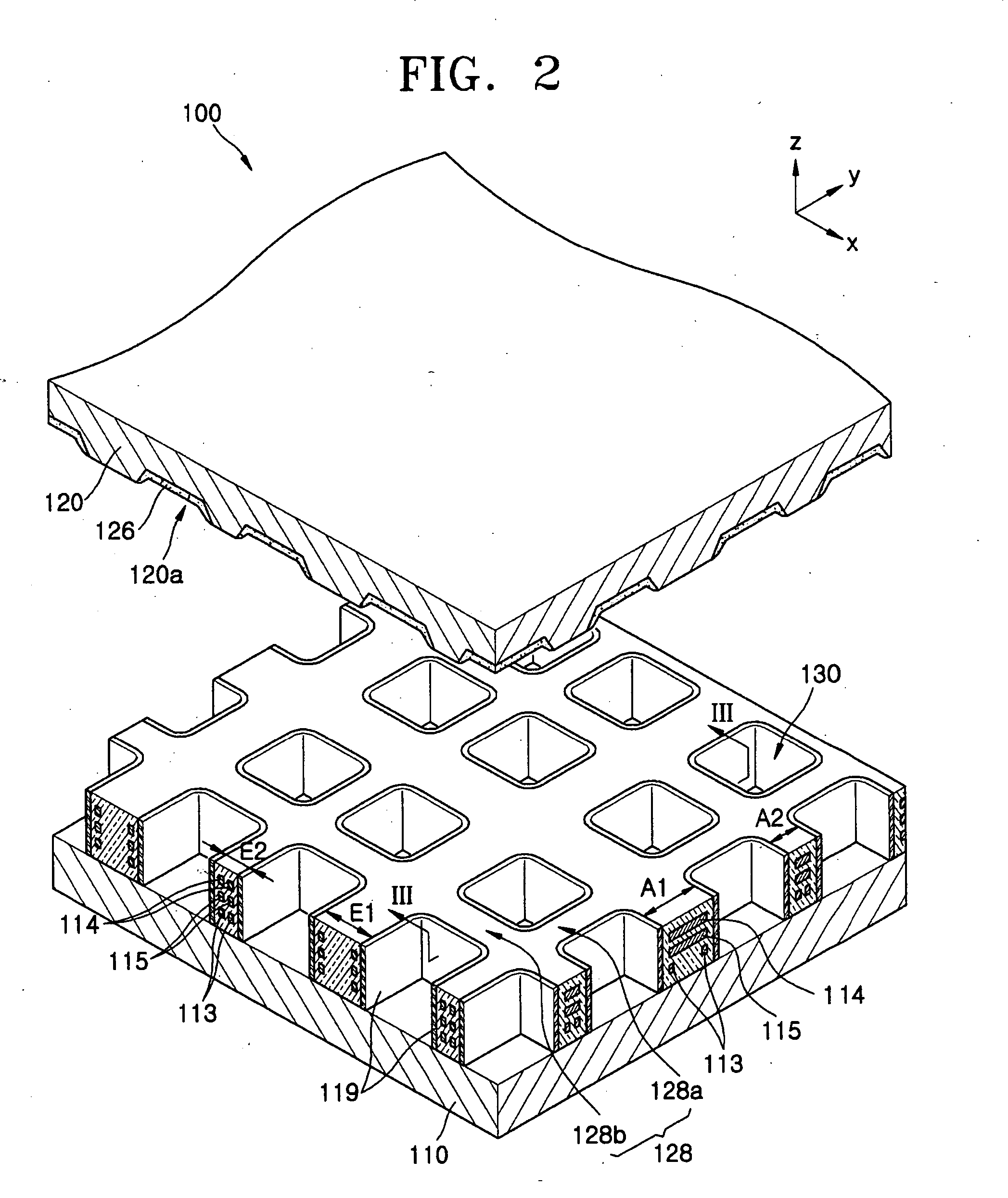
[0034] Turning now to FIGS. 2 through 6, FIG. 2 is an exploded perspective view of a plasma display panel 100 according to the present invention, and FIG. 3 is a cross-sectional view of the plasma display panel 100 of FIG. 2 taken along line III-III, FIG. 4 is a view of an arrangement of discharge cells and electrodes of the plasma display panel 100 of FIG. 2, FIG. 5 is a view of arrangements of discharge cells, sub-pixels, and unit pixels of the plasma display panel 100 of FIG. 2 taken along line V-V of FIG. 3 and FIG. 6 is a view of arrangements of the discharge cells, the sub-pixels, and the unit pixels of the plasma display panel 100 of FIG. 2 taken along line VI-VI of FIG. 3.

[0035] Referring now to FIGS. 2 and 3, the plasma display panel 100 includes a front substrate 120, phosphor layers 126, barrier ribs 128, first discharge electrodes 114, second discharge electrodes 115, address electrodes 113, a protective layer 119, and a rear substrate 110. The rear substrate 110 and the...

second embodiment

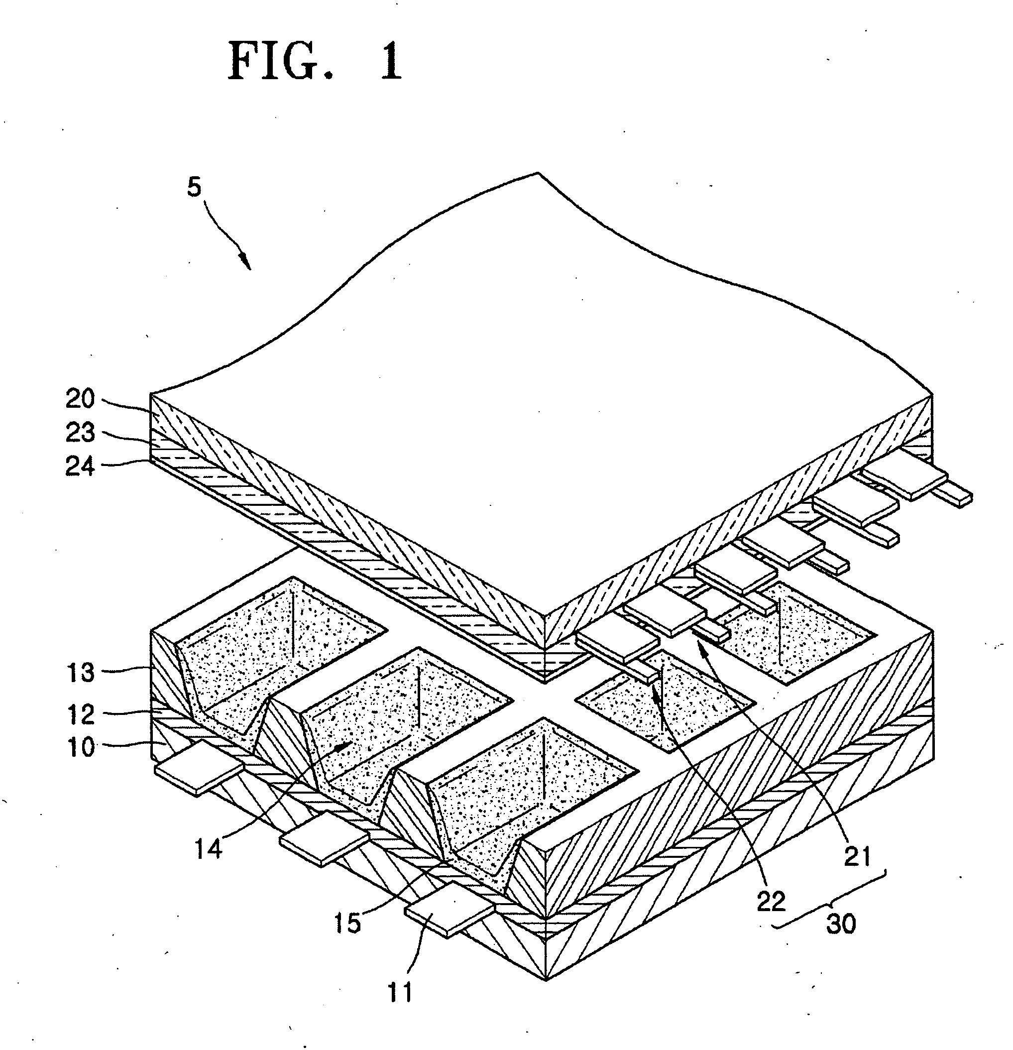
[0061] Turning now to FIGS. 8 through 10, FIGS. 8 through 10 illustrate a plasma display panel 200 according to the present invention. As illustrated in FIG. 8, the plasma display panel 200 includes a front substrate 220, phosphor layers 226, a rear substrate 210, barrier ribs 228, first discharge electrodes 214, second discharge electrodes 215 and address electrodes 213.

[0062] Within the barrier ribs 228 are the first discharge electrodes 214 and the second discharge electrodes 215 extending parallel to each other while surrounding the discharge cells 230 along the y direction. In the embodiment of FIGS. 8 through 10, address electrodes 213 are also arranged within barrier ribs 228 and surround rows of discharge cells 230 extending in the x direction crossing the first and second discharge electrodes 214,215 extending in the y direction. The barrier ribs 228 are made out of a dielectric material. The barrier ribs 228 can be broken down into transverse barrier ribs 228b extending in...


PUM


Abstract

Provided is a plasma display panel including a rear substrate, a front substrate separated from the rear substrate, a plurality of barrier ribs arranged between the front substrate and the rear substrate and adapted to define a plurality of discharge cells corresponding to a plurality of sub-pixels, a plurality of sustain electrode pairs comprising a plurality of first discharge electrodes and a plurality of second discharge electrodes extending parallel to each other and surrounding ones of the plurality of discharge cells, the plurality of sustain electrode pairs being adapted to generate a discharge, a plurality of address electrodes extending and surrounding the plurality of discharge cells and arranged in a direction that crosses the plurality of sustain electrode pairs, a plurality of phosphor layers arranged within the plurality of discharge cells and a discharge gas arranged within the plurality of discharge cells, wherein a predetermined number of sub-pixels form a unit pixel, and unit pixels adjacent to each other in a direction are spaced apart from each other by a predetermined distance.

Description

CLAIM OF PRIORITY [0001] This application makes reference to, incorporates the same herein, and claims all benefits accruing under U.S.C. §119 from an application for PLASMA DISPLAY PANEL earlier filed in the Korean Intellectual Property Office on 26 Apr. 2005 and there duly assigned Serial No. 10-2005-0034492. BACKGROUND OF THE INVENTION [0002] 1. Field of the Invention [0003] The present invention relates to a plasma display panel having a new structure. [0004] 2. Description of the Related Art [0005] Plasma display panels are flat panel displays displaying an image via gas discharge. Plasma display panels are considered to be the next generation of flat panel displays due to superior display properties such as display capacity, brightness, contrast, residual image, and wide viewing angle. The plasma display panel includes a rear substrate and a front substrate facing each other, spaced apart from each other and coupled to each other. A plurality of address electrodes are arranged...

Claims


Application Information

Patent Timeline
IPC IPC(8): H01J17/49H01J11/14H01J11/16H01J11/22H01J11/24H01J11/26H01J11/32H01J11/34H01J11/36H01J11/42
CPCH01J11/16H01J2211/365H01J11/36F26B3/347B30B9/02F26B2200/04B09B3/40
Inventor KANG, KYOUNG-DOO
Owner SAMSUNG SDI CO LTD
Why Eureka
Try Eureka