

NAND flash memory device and methods of its formation and operation
a flash memory and nand flash technology, applied in semiconductor devices, digital storage, instruments, etc., can solve problems such as inadvertent programming of selected cells b>10/b>, boosted channel voltage, etc., and achieve the effect of reducing the leakage curren
- Summary
- Abstract
- Description
- Claims
- Application Information
AI Technical Summary
Benefits of technology
Problems solved by technology
Method used
Image

Examples
first embodiment
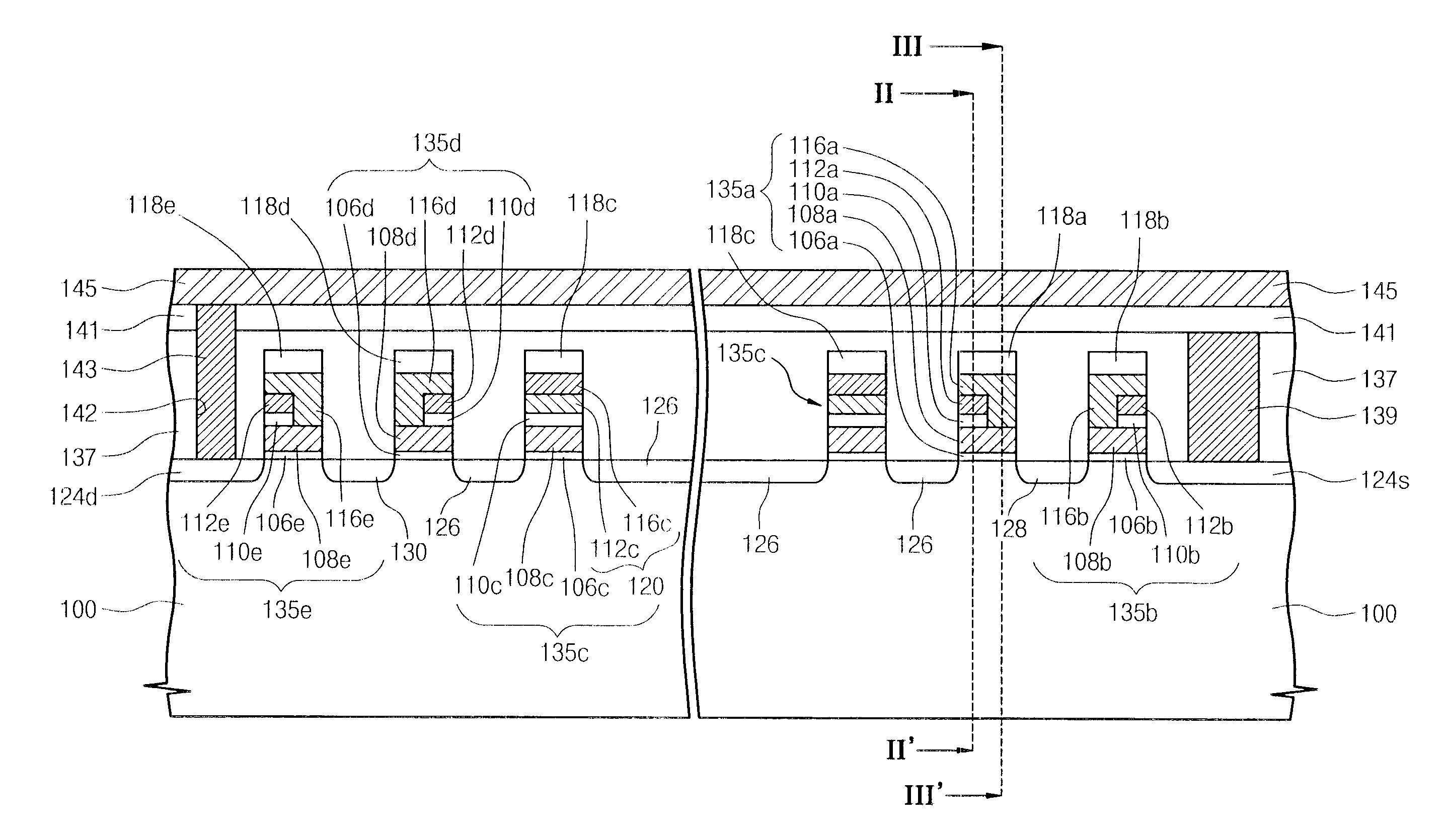
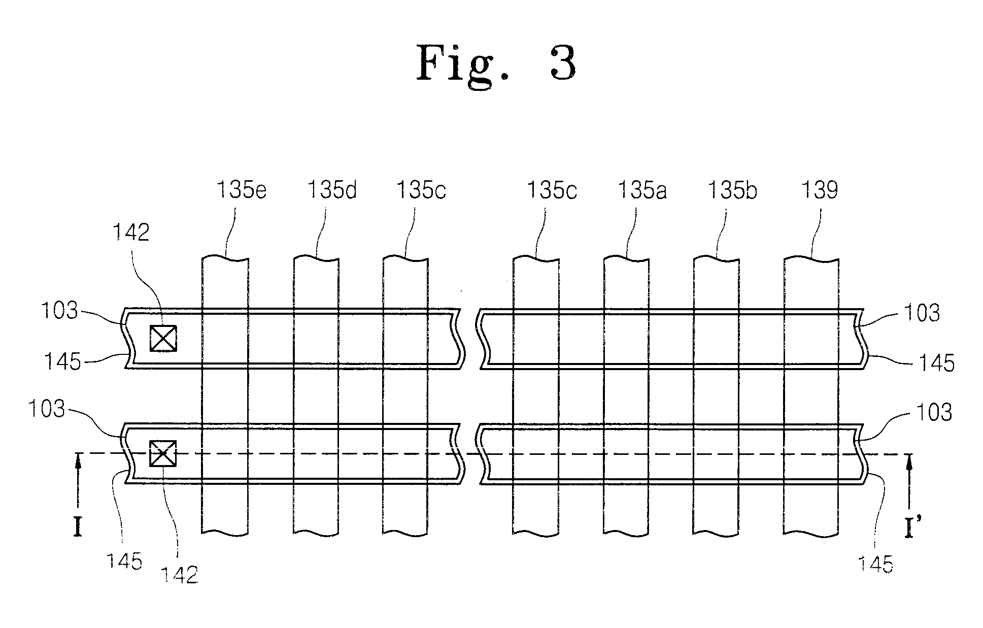
[0056]FIG. 3 is a plan view of a NAND flash memory device according to an embodiment of the present invention, FIG. 4A is a cross-sectional view taken along the line I-I′ of FIG. 3, and FIGS. 4B and 4C are cross-sectional views taken along the lines II-II′ and III-III′ of FIG. 4A, respectively.
[0057] Referring to FIGS. 3, and 4A through 4C, a device isolation layer 104 defining active regions 103 is disposed at a predetermined region of a semiconductor substrate 100. The active regions 103 are disposed in parallel with one another. The active regions 103 may be line-shaped. The device isolation layer 104 may fill a trench 102 formed in the semiconductor substrate 100. In other words, the device isolation layer 104 can be a trench type device isolation layer.
[0058] A plurality of cell gate lines 135c cross over the active regions 103. The plurality of cell gate lines 135c constitute a cell gate group. A first ground selection gate line 135a crosses over the active regions 103 dispo...
second embodiment
[0148]FIG. 14 is a plan view of a NAND flash memory device according to another embodiment of the present invention, and FIG. 15 is a cross-sectional view taken along the line IV-IV′ of FIG. 14.
[0149] Referring to FIGS. 14 and 15, a device isolation layer 204 defining active regions 203 is disposed at a predetermined region of a semiconductor substrate 200. The active regions 203 are disposed in parallel with one another.
[0150] A plurality of cell gate lines 230c cross over the active regions 203 in parallel. The plurality of cell gate lines 230c constitute a cell gate group. First and second ground selection gate lines 230a and 230b are sequentially disposed at one side of the cell gate group. The first and second ground selection gate lines 230a and 230b cross the active regions 203 in parallel and are spaced apart from each other.
[0151] A first string selection gate line 230d is disposed at the other side of the cell gate group and crosses over the active regions 203 of an opp...
third embodiment
[0215] The present embodiment discloses first and second ground selection transistors different than those of the first and second embodiments. According to the present embodiment, channel regions of the first and second ground selection transistors are directly connected with each other.
[0216]FIG. 23 is an equivalent circuit diagram of a NAND flash memory device according to another embodiment of the present invention.
[0217] Referring to FIG. 23, a plurality of cell strings are arranged in parallel. Each of the cell strings includes a cell group consisting of a plurality of cell transistors ‘CT’ connected in series. The cell transistor ‘CT’ includes a charge storage means. First and second ground selection transistors ‘GST1 and GST2’ are sequentially connected in series to one end of the cell group. First and second string selection transistors ‘SST1 and SST2’ are sequentially connected in series to the other end of the cell group. In further detail, the first ground selection tr...
PUM
 Abstract
Description
Claims
Application Information