Cleaning method and cleaning apparatus
a cleaning method and cleaning technology, applied in the field of cleaning methods and cleaning equipment, can solve problems such as unsuitable for actual us
- Summary
- Abstract
- Description
- Claims
- Application Information
AI Technical Summary
Benefits of technology
Problems solved by technology
Method used
Image


Examples
first embodiment
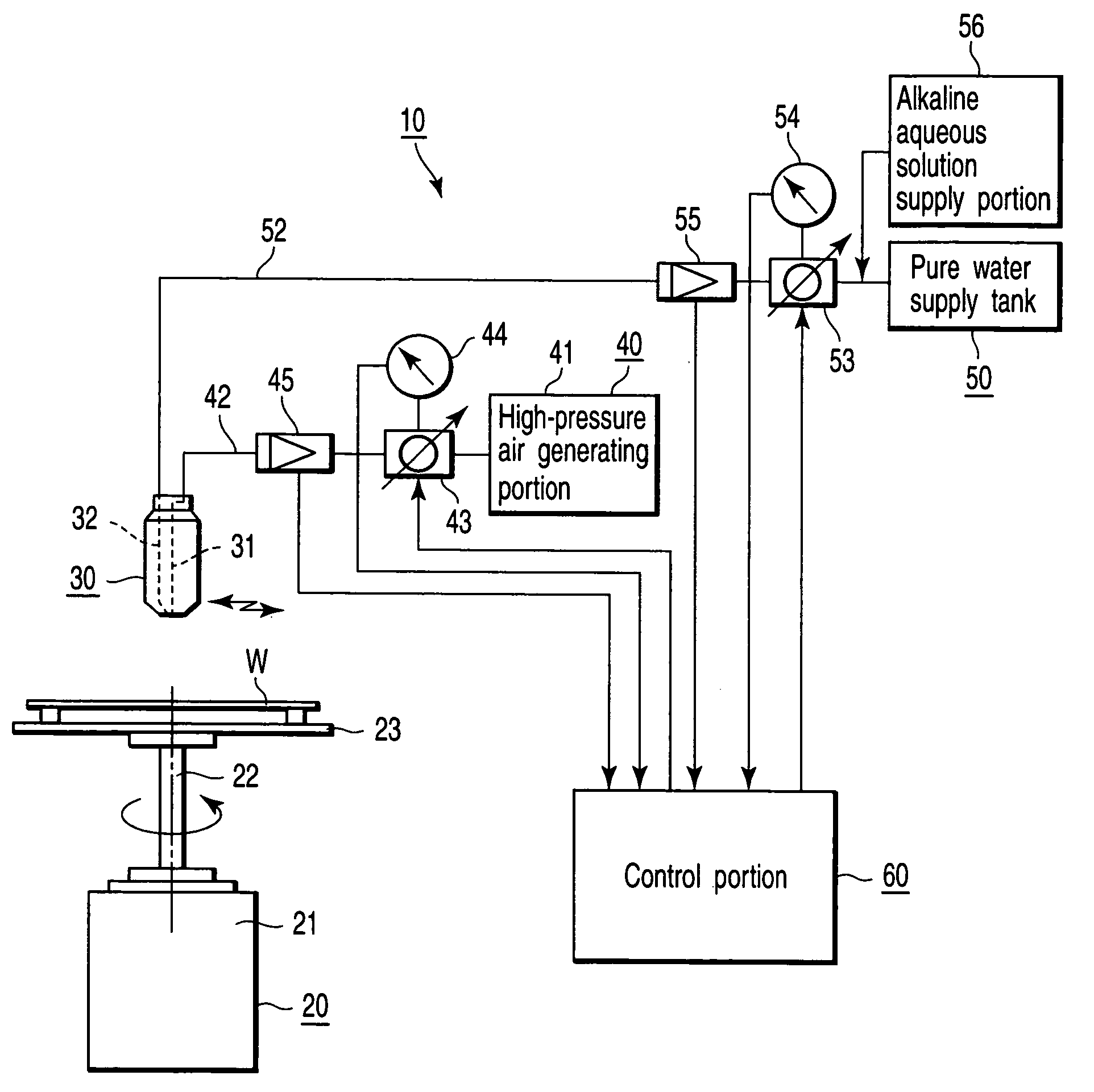
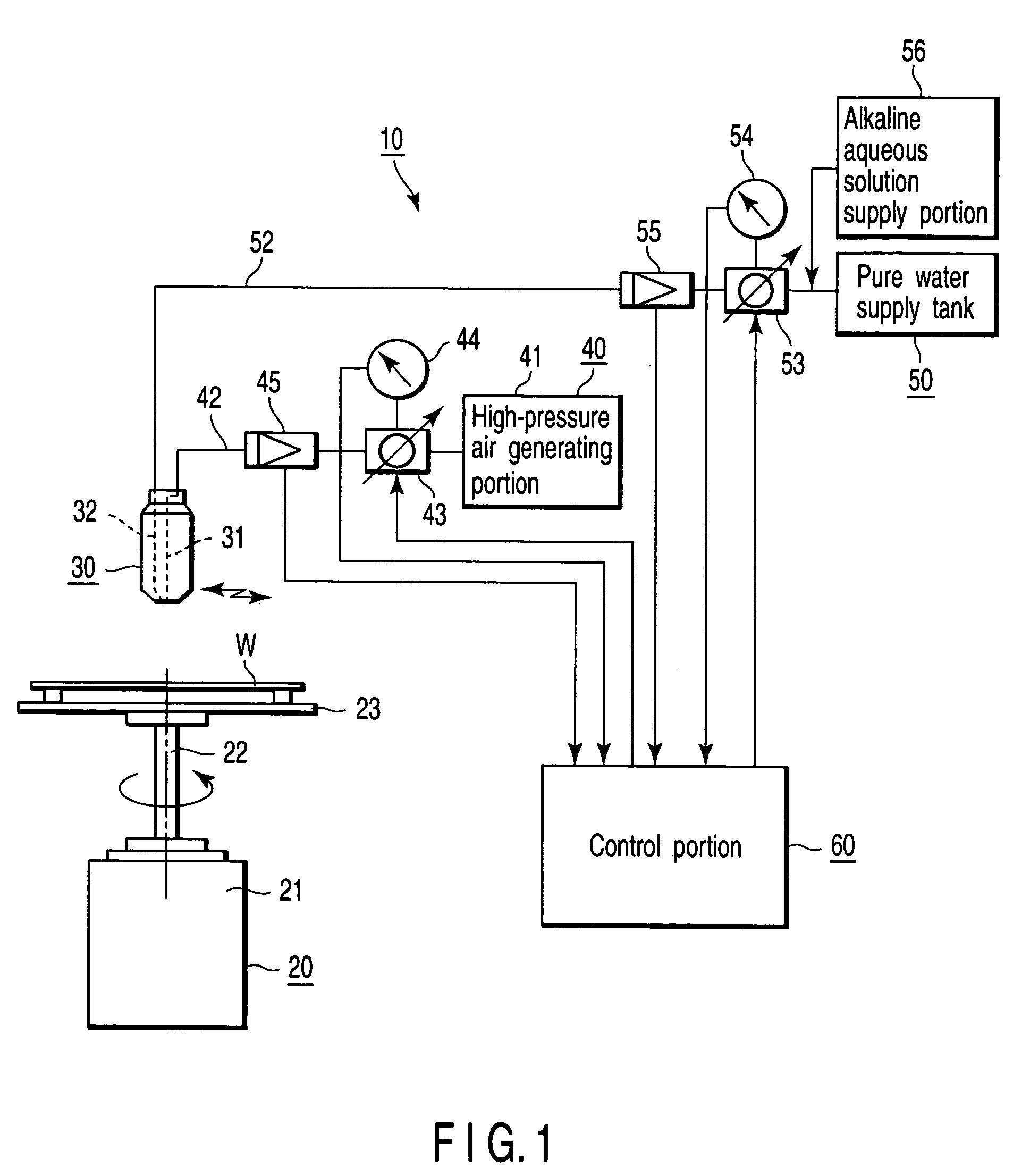
[0036]FIG. 1 is an explanatory diagram showing the structure of a substrate cleaning apparatus 10 according to the present invention and FIGS. 2 to 5 are explanatory diagrams showing the reason why alkali aqueous solution is used in the substrate cleaning apparatus 10.
[0037] The substrate cleaning apparatus 10 comprises a cleaning portion 20, a high-pressure air supply portion 40, a cleaning water supply portion 50 and a control portion 60 for controlling these portions in harmony with each other.
[0038] The cleaning portion 20 comprises an electric motor 21 which is controlled by the control portion 60, a spin chuck 23 which is mounted on a rotation shaft 22 of this electric motor 21 for holding a semiconductor wafer W, and a two-fluid nozzle 30 disposed to oppose the spin chuck 23. The two-fluid nozzle 30 includes a gas passage 31 through which high-pressure air flows which is disposed in the center and a cleaning water passage 32 which is disposed around this gas passage 31 and t...
second embodiment
[0051]FIG. 6 is an explanatory diagram showing the structure of a substrate cleaning apparatus 110 according to the present invention and FIGS. 7, 8 are diagrams showing the relation between the flow rate of nitrogen in the substrate cleaning apparatus 110 and the quantity of damages of the device pattern.
[0052] The substrate cleaning apparatus 110 comprises a cleaning portion 120, a high-pressure nitrogen supply portion 140, a cleaning water supply portion 150 and a control portion 160 for controlling these components in harmony with each other.
[0053] The cleaning portion 120 includes an electric motor 121 which is controlled by the control portion 160, a spin chuck 123 which is mounted on a rotation shaft 122 of this electric motor 121 for holding a semiconductor wafer W, and a two-fluid nozzle 130 which is disposed to oppose the spin chuck 123.
[0054] The two-fluid nozzle 130 comprises, as shown in FIG. 7, a nozzle main body 131 which is grounded, a gas passage 132 which is prov...
third embodiment
[0066]FIG. 9 is an explanatory diagram showing the structure of a substrate cleaning apparatus 210 according to the present invention. FIGS. 10 and 11 are diagrams showing the relation between the flow rate of nitrogen in the substrate cleaning apparatus 210 and the quantity of damages in the device pattern.
[0067] The substrate cleaning apparatus 210 comprises a cleaning portion 220, a high-pressure nitrogen supply portion 240, a cleaning water supply portion 250 and a control portion 260 for controlling these components in harmony with each other.
[0068] The cleaning portion 220 comprises an electric motor 221 which is controlled by the control portion 260, a spin chuck 223 which is mounted on a rotation shaft 222 of this electric motor 221 to hold the semiconductor wafer W, and a two-fluid nozzle 230 disposed to oppose the spin chuck 223. The two-fluid nozzle 230 includes a gas passage 231 through which high-pressure nitrogen passes in the center, and a cleaning water passage 232 ...
PUM
 Abstract
Description
Claims
Application Information
 - Generate Ideas
- Intellectual Property
- Life Sciences
- Materials
- Tech Scout
- Unparalleled Data Quality
- Higher Quality Content
- 60% Fewer Hallucinations
Browse by: Latest US Patents, China's latest patents, Technical Efficacy Thesaurus, Application Domain, Technology Topic, Popular Technical Reports.
© 2025 PatSnap. All rights reserved.Legal|Privacy policy|Modern Slavery Act Transparency Statement|Sitemap|About US| Contact US: help@patsnap.com