Thin film transistor panel, liquit crystal display having the same and method of manufacturing the thin film transistor panel

a technology of thin film transistors and liquit crystal displays, applied in non-linear optics, instruments, optics, etc., can solve the problems of high precision and expensive exposure equipment in the process of forming the color filter on the lower panel, and achieve the effect of improving structure, cheaper and simpler manufacturing process

Active Publication Date: 2006-11-09
SAMSUNG DISPLAY CO LTD
View PDF5 Cites 26 Cited by
  • Summary
  • Abstract
  • Description
  • Claims
  • Application Information

AI Technical Summary

Benefits of technology

[0013] The present invention provides a thin film transistor (TFT) panel having an improved structure, which has a cheaper and simpler manufacturing process, an LCD having the same, and a method of manufacturing the TFT panel.

Problems solved by technology

However, COA is disadvantageous in that a process of forming the color filter on the lower panel requires high precision, expensive exposure equipment.

Method used


Image

  • Thin film transistor panel, liquit crystal display having the same and method of manufacturing the thin film transistor panel
  • Thin film transistor panel, liquit crystal display having the same and method of manufacturing the thin film transistor panel
  • Thin film transistor panel, liquit crystal display having the same and method of manufacturing the thin film transistor panel

Examples


Embodiment Construction

[0028] Advantages and features of the present invention and methods of accomplishing the same may be understood more readily by reference to the following detailed description of preferred embodiments and the accompanying drawings. The present invention may, however, be embodied in many different forms and should not be construed as being limited to the embodiments set forth herein. Rather, these embodiments are provided so that this disclosure will be thorough and complete and will fully convey the concept of the invention to those skilled in the art, and the present invention will only be defined by the appended claims. Like reference numerals refer to like elements throughout the specification.

[0029] The present invention will now be described more fully with reference to the accompanying drawings, in which preferred embodiments of this invention are shown.

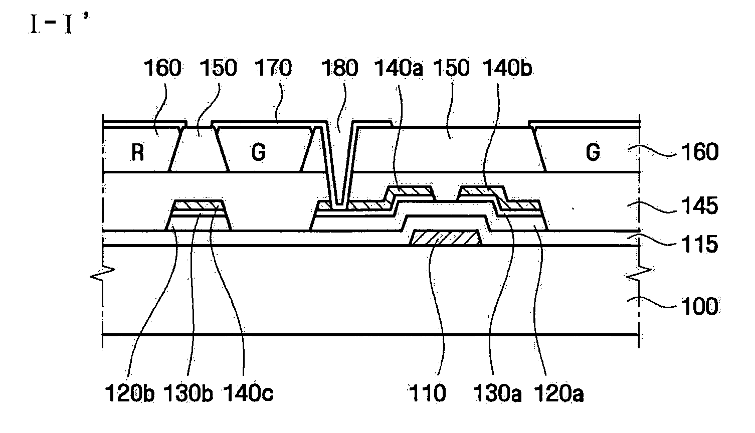
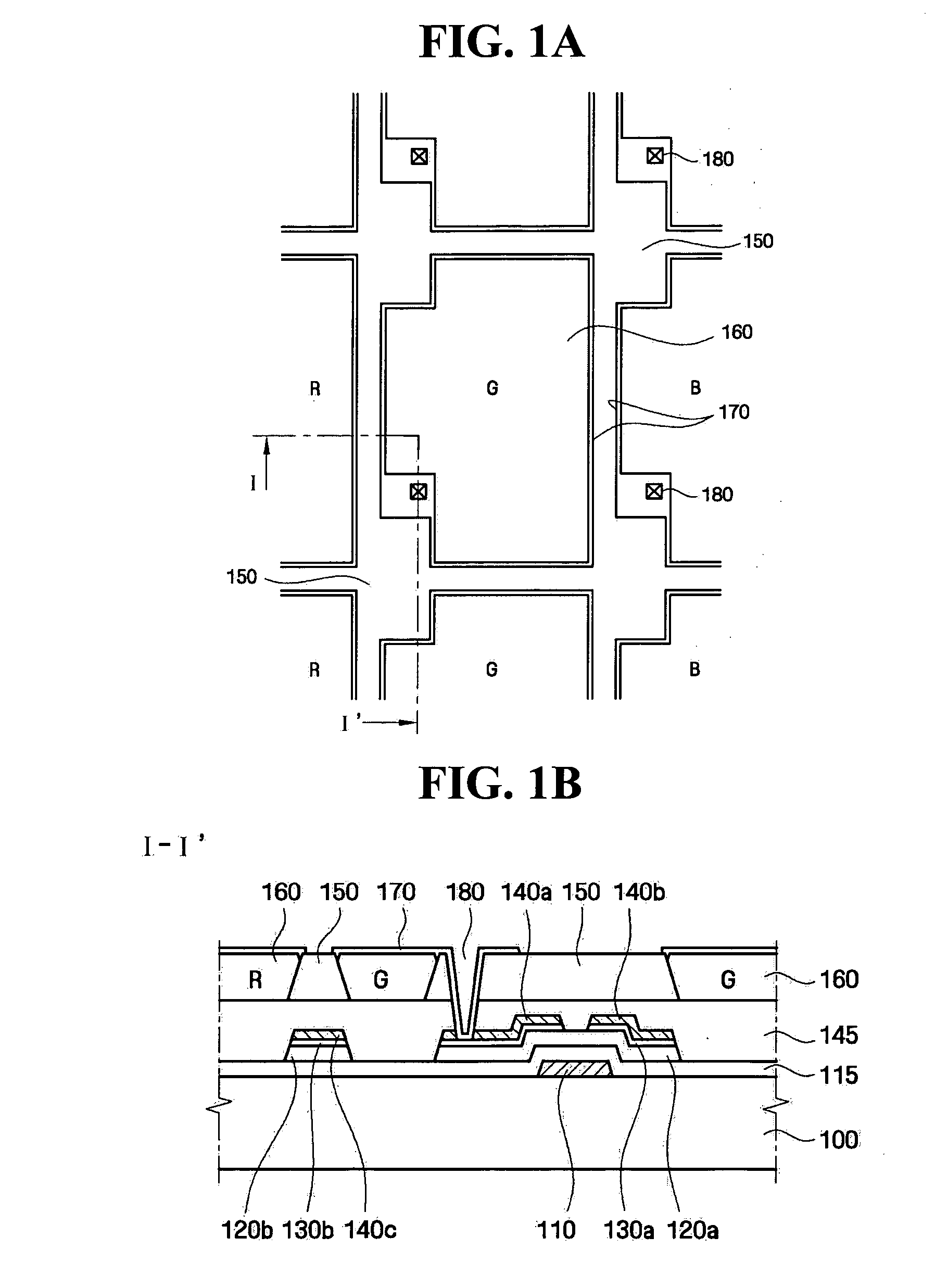
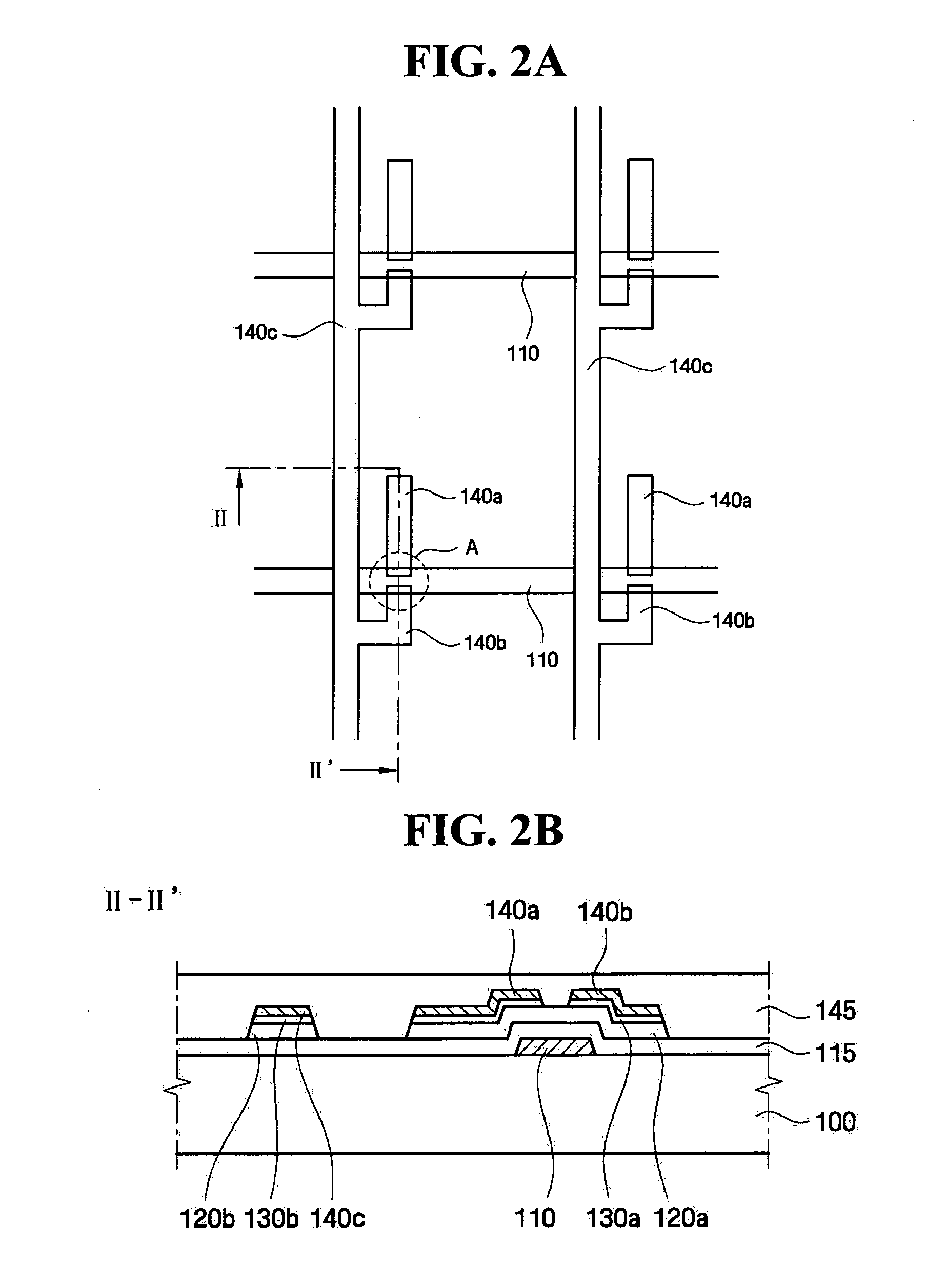
[0030]FIGS. 1A and 1B are a layout view and a partial cross-sectional view, respectively, of a thin film transistor (TFT) p...


PUM

PropertyMeasurementUnit
non-hygroscopicaaaaaaaaaa
heightaaaaaaaaaa
hollow shapeaaaaaaaaaa

Abstract

A thin film transistor panel, a liquid crystal display having the same, and a method of manufacturing the thin film transistor panel are provided. The thin film transistor includes a gate line formed on an insulating substrate in a predetermined direction, a data line crossing the gate line, a thin film transistor connected to the gate line and the data line, a black matrix formed to overlap at least a portion of the gate line, the data line, and the thin film transistor, a color filter formed in a region partitioned by the black matrix, and a pixel electrode formed on the color filter and electrically connected to the thin film transistor.

Description

[0001] This application claims priority from Korean Patent Application No. 10-2005-0038058 filed on May 6, 2005 in the Korean Intellectual Property Office, the disclosure of which is incorporated herein by reference in its entirety. BACKGROUND OF THE INVENTION [0002] 1. Field of the Invention [0003] The present invention relates to a thin film transistor (hereinafter referred to as a TFT) panel, a liquid crystal display (hereinafter referred to as an LCD) having the same, and a method of manufacturing the TFT panel, and more particularly, to a TFT panel for an LCD, which has an improved structure and a simpler and cheaper manufacturing process, an LCD having the same, and a method of manufacturing the TFT panel. [0004] 2. Description of the Related Art [0005] Recently, LCDs have been widely used as display units. [0006] In a liquid crystal display device, when a voltage is applied to a liquid crystal cell, a molecular arrangement of the liquid crystal is changed to cause a change in...

Claims


Application Information

Patent Timeline
Patent Type & Authority Applications(United States)
IPC IPC(8): G02F1/136G02F1/1335
CPCG02F1/136209G02F2001/136222G02F1/136227G02F1/136222G02F1/1335
Inventor KIM, JANG-SOO
Owner SAMSUNG DISPLAY CO LTD
Why Eureka
Try Eureka