Semiconductor integrated circuit device which executes data transfer between a plurality of devices connected over network, and data transfer method

Inactive Publication Date: 2006-11-09
KK TOSHIBA
View PDF3 Cites 5 Cited by
  • Summary
  • Abstract
  • Description
  • Claims
  • Application Information

AI Technical Summary

Benefits of technology

[0015] causing a control circuit to confirm completion of the read-out of the transfer data into the first buffer circuit, and to acquire a right of use of the data bus;
[0016] causing the control circuit to transfer the tr

Problems solved by technology

In these prior-art data transfer methods, howe

Method used


Image

  • Semiconductor integrated circuit device which executes data transfer between a plurality of devices connected over network, and data transfer method
  • Semiconductor integrated circuit device which executes data transfer between a plurality of devices connected over network, and data transfer method
  • Semiconductor integrated circuit device which executes data transfer between a plurality of devices connected over network, and data transfer method

Examples


first embodiment

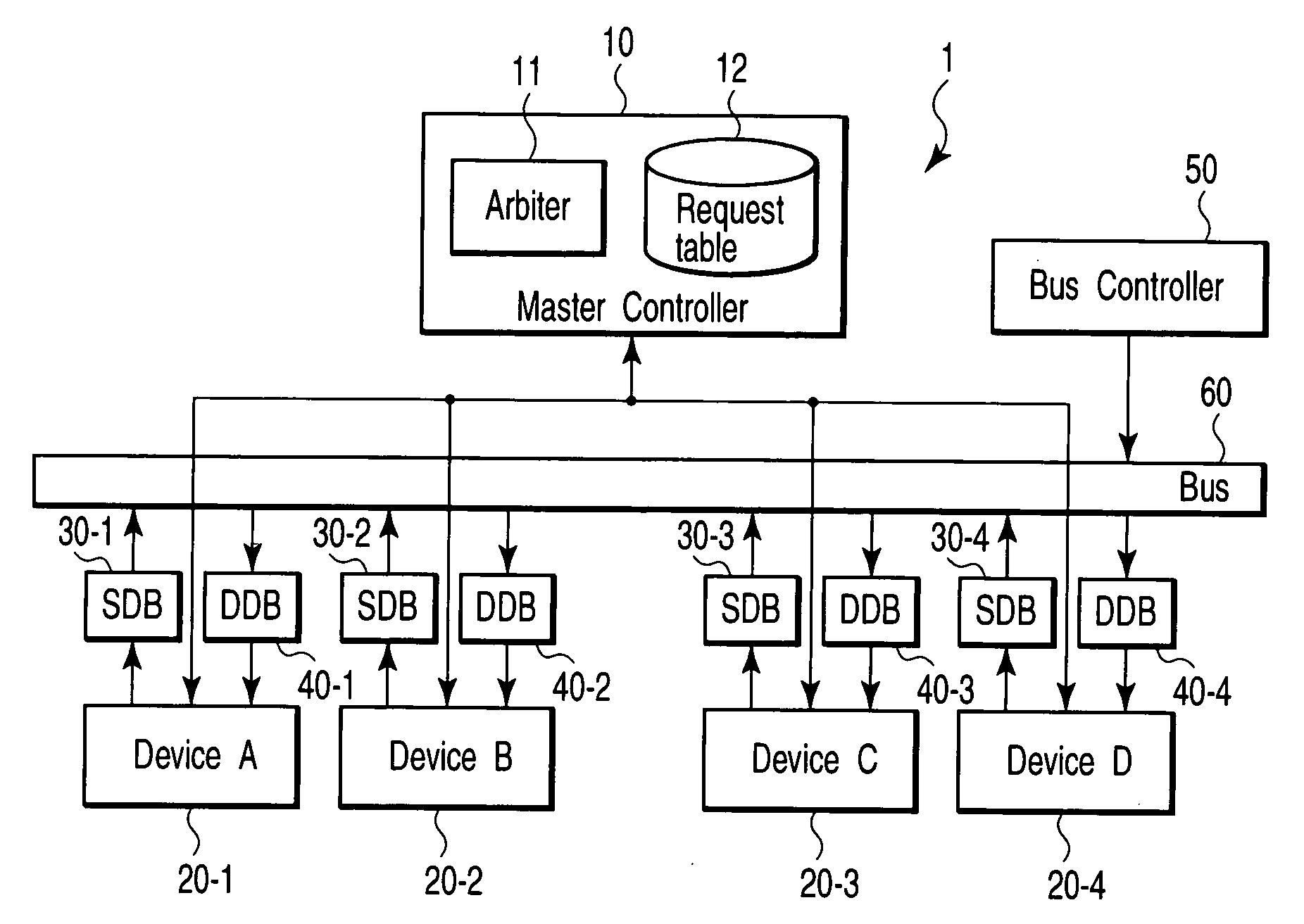
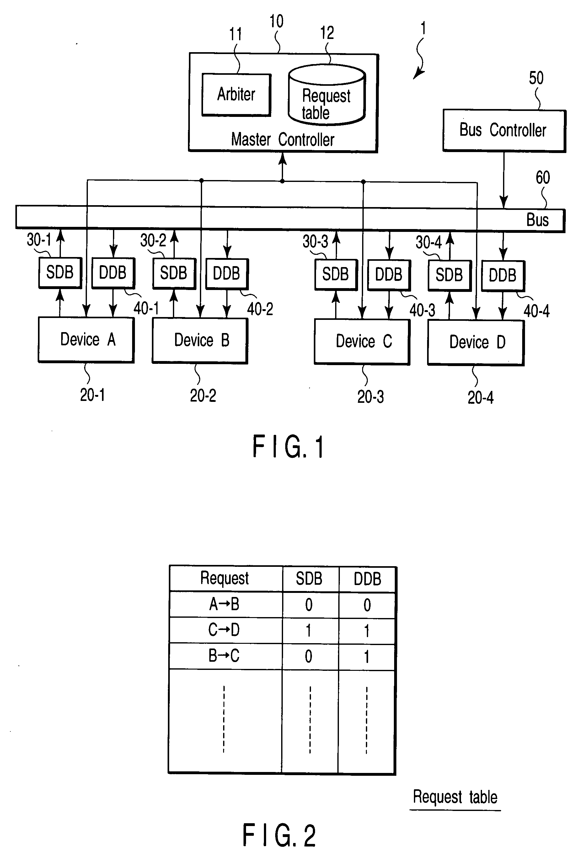
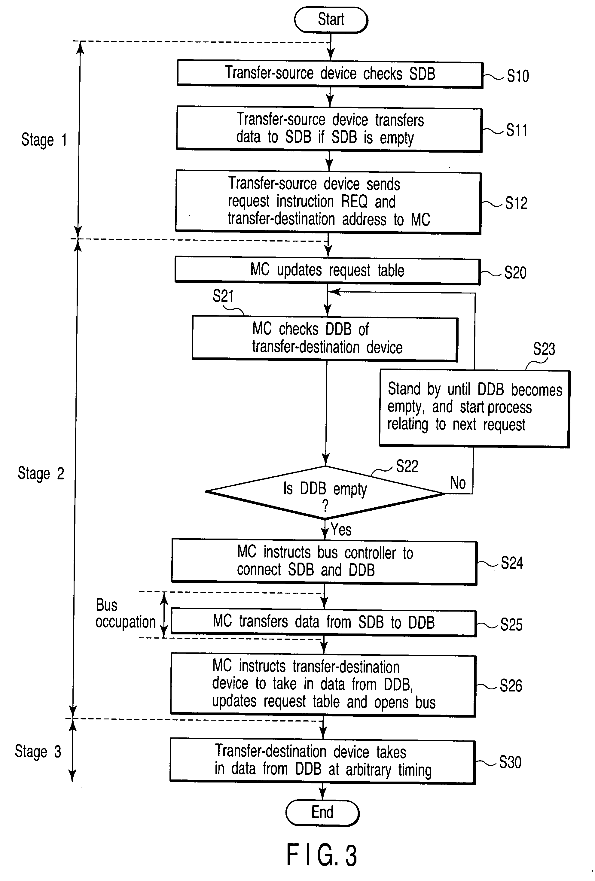
[0052] A semiconductor integrated circuit device and a data transfer method according to the present invention will now be described with reference to FIG. 1. FIG. 1 is a block diagram of a semiconductor integrated circuit (LSI) according to this embodiment. As is shown in FIG. 1, an LSI 1 comprises a master controller (hereinafter abbreviated as “MC”) 10, four semiconductor devices 20-1 to 20-4 (hereinafter referred to as “devices A to D”), source data buffers (SDB) 30-1 to 30-4, destination data buffers (DDB) 40-1 to 40-4, a bus controller 50, and a data bus 60.

[0053] The devices A to D are independent semiconductor devices, and each of the devices A to D includes a CPU, a memory and an input / output circuit. The devices A to D execute mutual data transmission / reception via a data bus 60. It should suffice if each of the devices A to D has a data transfer function, and the structure of devices A to D is not limited to the above-described one.

[0054] The SDBs 30-1 to 30-4 are provid...

second embodiment

[0096] Next, a semiconductor integrated circuit device and a data transfer method according to the present invention are described with reference to FIG. 11. FIG. 11 is a block diagram of an LSI according to this embodiment. The present embodiment relates to a case in which the MC 10 receives a request instruction from a block other than the devices A to D.

[0097] As is shown in FIG. 11, the LSI 1 of this embodiment further comprises a host processor 70 in addition to the structure shown in FIG. 1, which has been described in connection with the first embodiment. The host processor 70 issues a request for data transfer between devices A to D to the MC 10, and outputs a request instruction to the MC 10.

[0098] A data transfer method executed by the LSI 1 of this embodiment is described with reference to FIG. 12. FIG. 12 is a flow chart illustrating the data transfer method according to this embodiment.

[0099] To start with, the process in the stage 1 is executed. The host processor 70...

fourth embodiment

[0157] With the LSI according to the above-described fourth embodiment of the invention, the following advantageous effect (7) can be obtained in addition to the advantageous effects (1) to (6).

[0158] (7) The Data Transfer Efficiency can be Improved (Part 5).

[0159] According to the structure of the fourth embodiment, each of the SDB and DDB includes a plurality of entries and thus can store a plurality of transfer data. The MC 10 can optimally alter the order of transfer of data read out into the SDB by the transfer-source device. In addition, the transfer-destination device can take in the plural data, which are stored in the DDB, in the optimal order. The data transfer in the out-of-order fashion can be implemented, and the standby time for the execution of transfer can be reduced. Therefore, the transfer efficiency can be enhanced.

[0160] Next, a semiconductor integrated circuit device and a data transfer method according to a fifth embodiment of the present invention are descri...


PUM


Abstract

A semiconductor integrated circuit device includes a first semiconductor device and a second semiconductor device, first and second buffer circuits, a data bus, and a control circuit. The semiconductor integrated circuit device executes data transmission/reception between the first and second semiconductor devices. The first and second buffer circuits store data. The data bus transmits the data between the first and second buffer circuits. The first semiconductor device reads out the transfer data into the first buffer circuit. The control circuit transfers the transfer data, which is stored in the first buffer circuit, to the second buffer circuit via the data bus. The control circuit acquires a right of use of the data bus after the first semiconductor device writes the transfer data into the first buffer circuit, and disclaims the right of use of the data bus after the transfer data is transferred to the second buffer circuit.

Description

CROSS-REFERENCE TO RELATED APPLICATIONS [0001] This application is based upon and claims the benefit of priority from prior Japanese Patent Application No. 2005-136150, filed May 9, 2005, the entire contents of which are incorporated herein by reference. BACKGROUND OF THE INVENTION [0002] 1. Field of the Invention [0003] The present invention relates generally to a semiconductor integrated circuit device and a data transfer method, and relates to, for instance, a data transfer scheme of data transfer between a plurality of devices connected over a network. [0004] 2. Description of the Related Art [0005] In recent years, the amount of data handled in computers has been increasing with great rapidity. Accordingly, how to increase a data transfer speed is very important from the standpoint of enhancement in processing speed of computers. [0006] In the prior art, Jpn. Pat. Appln. KOKAI Publication No. 2001-209626 and Jpn. Pat. Appln. KOKAI Publication No. H10-116244, for instance, discl...

Claims


Application Information

Patent Timeline
IPC IPC(8): G06F5/00
CPCG06F13/362
Inventor KATAYAMA, YASUHIROGOTO, HARUTAKA
Owner KK TOSHIBA
Why Eureka
Try Eureka