Trenched-gate field effect transistors and methods of forming the same

a field effect transistor and transistor technology, applied in the direction of semiconductor devices, diodes, electrical apparatus, etc., can solve the problems of reducing the efficiency of the transistor, so as to achieve the effect of improving the voltage performance of the transistor and maintaining a low rdson

Active Publication Date: 2006-11-30
SEMICON COMPONENTS IND LLC
View PDF99 Cites 180 Cited by
  • Summary
  • Abstract
  • Description
  • Claims
  • Application Information

AI Technical Summary

Benefits of technology

[0008] In accordance with one embodiment of the invention, a monolithically integrated field effect transistor and Schottky diode includes gate trenches extending into a semiconductor region. Source regions having a substantially triangular shape flank each side of the gate trenches. A contact opening extends into the semiconductor region between adjacent gate trenches. A conductor layer fills the contact opening to electrically contact: (a) the source regions along at least a portion of a slanted sidewall of each source region, and (b) the semiconductor region along a bottom portion of the contact opening, wherein the conductor layer forms a Schottky contact with the semiconductor region.

Problems solved by technology

For example, in the case of the power MOSFET, because of the proportional relationship between the drain-to-source on-resistance RDSon and the breakdown voltage, improving the voltage performance of the transistor while maintaining a low RDSon poses a challenge.
A drawback of conventional accumulation transistors is that the drift region needs to be lightly doped to support a high enough reverse bias voltage.
However, a lightly doped drift region results in a higher on-resistance and lower efficiency.
Similarly, in enhancement mode FETs, improving the transistor break down voltage often comes at the price of higher on-resistance or vice versa.

Method used


Image

  • Trenched-gate field effect transistors and methods of forming the same
  • Trenched-gate field effect transistors and methods of forming the same
  • Trenched-gate field effect transistors and methods of forming the same

Examples


Embodiment Construction

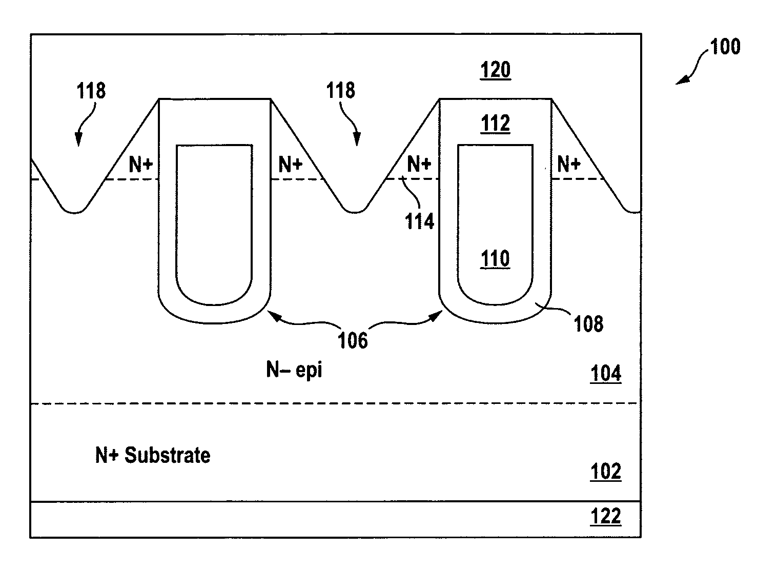
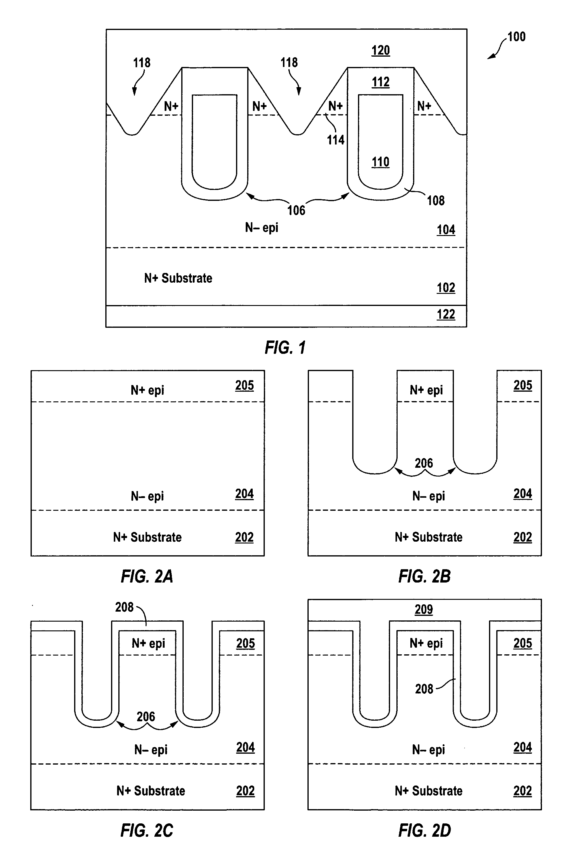
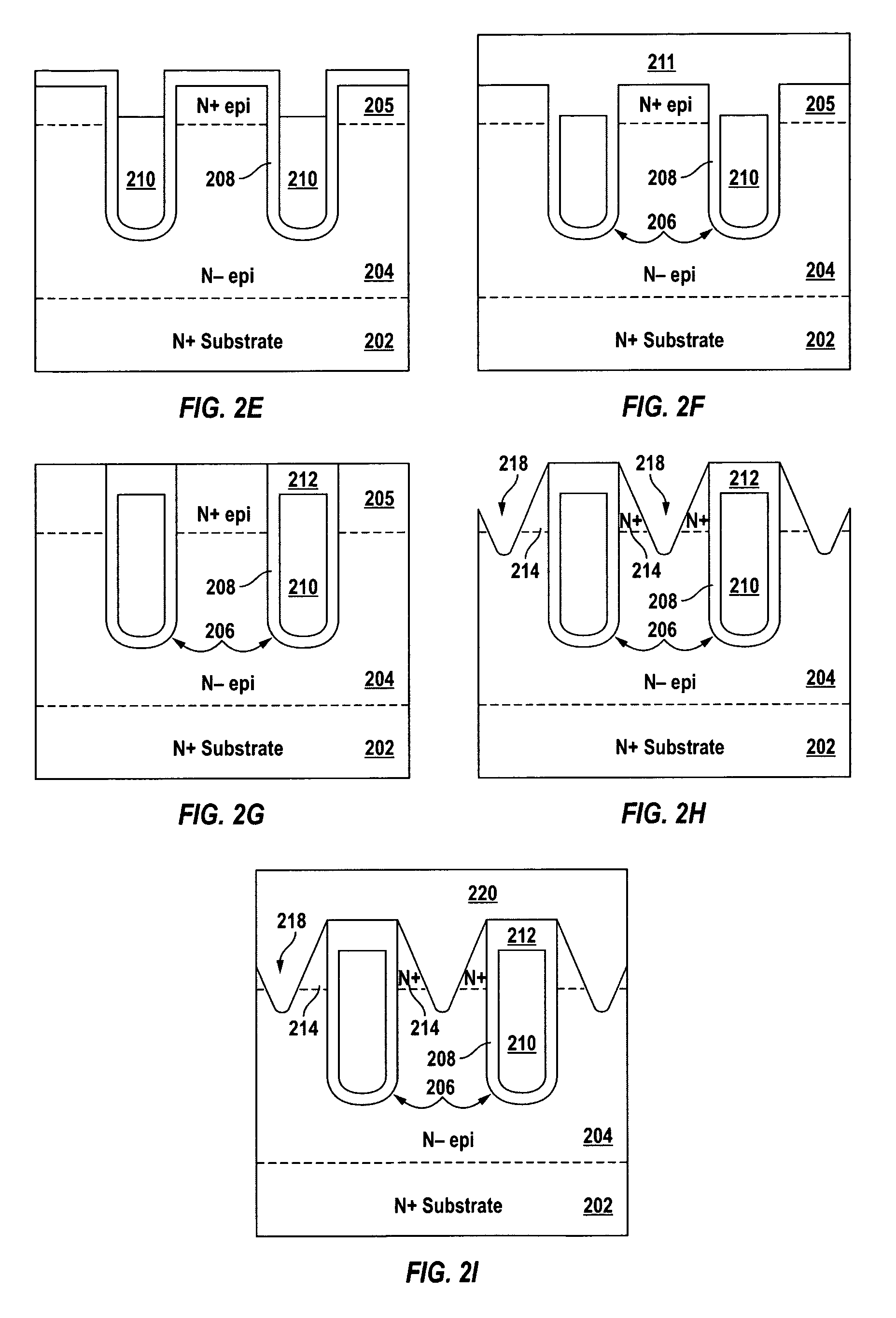
[0041] The power switch can be implemented by any one of power MOSFET, IGBT, various types of thyristors and the like. Many of the novel techniques presented herein are described in the context of the power MOSFET for illustrative purposes. It is to be understood however that the various embodiments of the invention described herein are not limited to the power MOSFET and can apply to many of the other types of power switch technologies, including, for example, IGBTs and other types of bipolar switches. Further, for the purposes of illustration, the various embodiments of the invention are shown to include specific p and n type regions. It is understood by those skilled in the art that the teachings herein are equally applicable to devices in which the conductivities of the various regions are reversed.

[0042]FIG. 1 shows a simplified cross section view of a trenched-gate accumulation field effect transistor (FET) optimally integrated with a Schottky diode in a single cell, in accor...


PUM


Abstract

A monolithically integrated field effect transistor and Schottky diode includes gate trenches extending into a semiconductor region. Source regions having a substantially triangular shape flank each side of the gate trenches. A contact opening extends into the semiconductor region between adjacent gate trenches. A conductor layer fills the contact opening to electrically contact: (a) the source regions along at least a portion of a slanted sidewall of each source region, and (b) the semiconductor region along a bottom portion of the contact opening, wherein the conductor layer forms a Schottky contact with the semiconductor region.

Description

CROSS-REFERENCES TO RELATED APPLICATIONS [0001] This application claims the benefit of U.S. Provisional Application No. 60 / 669,063, filed Apr. 6, 2005, and is incorporated herein by reference in its entirety for all purposes. The following patent applications are incorporated herein by reference in their entirety for all purposes: U.S. Provisional Application No. 60 / 588,845, filed Jul. 15, 2004, U.S. application Ser. No. 11 / 026,276, filed Dec. 29, 2004, and U.S. application Ser. No. 09 / 844,347, filed Apr. 27, 2001 (Publication No. U.S. 2002 / 0008284).BACKGROUND OF THE INVENTION [0002] The present invention relates in general to power semiconductor technology, and more particularly to accumulation-mode and enhancement-mode trenched-gate field effect transistors (FETs) and their methods of manufacture. [0003] The key component in power electronic applications is the solid state switch. From ignition control in automotive applications to battery-operated consumer electronic devices, to ...

Claims


Application Information

Patent Timeline
Patent Type & Authority Applications(United States)
IPC IPC(8): H01L29/76
CPCH01L21/26586H01L29/7827H01L29/0619H01L29/0847H01L29/1095H01L29/407H01L29/41766H01L29/42368H01L29/66666H01L29/66719H01L29/66727H01L29/66734H01L29/7806H01L29/7811H01L29/7813H01L29/7828H01L29/872H01L2924/13091H01L27/0629H01L29/0869
Inventor SAPP, STEVENYILMAZ, HAMZAREXER, CHRISTOPHER LAWRENCECALAFUT, DANIEL
Owner SEMICON COMPONENTS IND LLC
Why Eureka
Try Eureka