Liquid crystal device and electronic apparatus

a liquid crystal device and electronic equipment technology, applied in static indicating devices, non-linear optics, instruments, etc., can solve the problems of difficult to obtain favorable display for both reflective display and transmisive display, and achieve easy matching of electro-optical characteristics, low cost, and the effect of favorable display

Inactive Publication Date: 2006-11-30
JAPAN DISPLAY WEST
View PDF12 Cites 90 Cited by
  • Summary
  • Abstract
  • Description
  • Claims
  • Application Information

AI Technical Summary

Benefits of technology

[0011] According to this configuration, it is possible to implement an FFS-mode liquid crystal device which can perform favorable display for both reflective display and transmissive display.
[0012] In the liquid crystal device according to the first aspect of the invention, of the strip electrodes, the one or more strip electrodes arranged in the transmissive display region may have a width larger than that of the one or more strip electrodes arranged in the reflective display region. With this configuration, the inter-electrode gap can be easily performed by adjusting the line widths of the strip electrodes. Therefore, the adjustment for optimization of optical conditions can be easily performed.
[0013] In the liquid crystal device according to the first aspect of the invention, it is preferable that a product dt×Gt of the gap dt between the electrodes in the electric field direction in the transmissive d

Problems solved by technology

Accordingly, it is difficult to obtain favorable display for both reflective

Method used


Image

  • Liquid crystal device and electronic apparatus
  • Liquid crystal device and electronic apparatus
  • Liquid crystal device and electronic apparatus

Examples


first embodiment

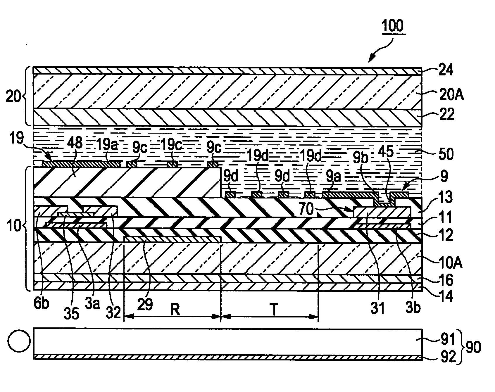
[0028] Hereinafter, a liquid crystal device according to a first embodiment of the invention will be described with reference to the drawings. The liquid crystal device of this embodiment is a transverse electric field mode liquid crystal device which performs image display by applying an electric field (transverse electric field) along a surface of a substrate to a liquid crystal layer and performing alignment control, in particular, an IPS (In-Plane Switching) mode liquid crystal device.

[0029] The scale of each layer or member has been adjusted in order to have a recognizable size in the drawings related to the embodiments.

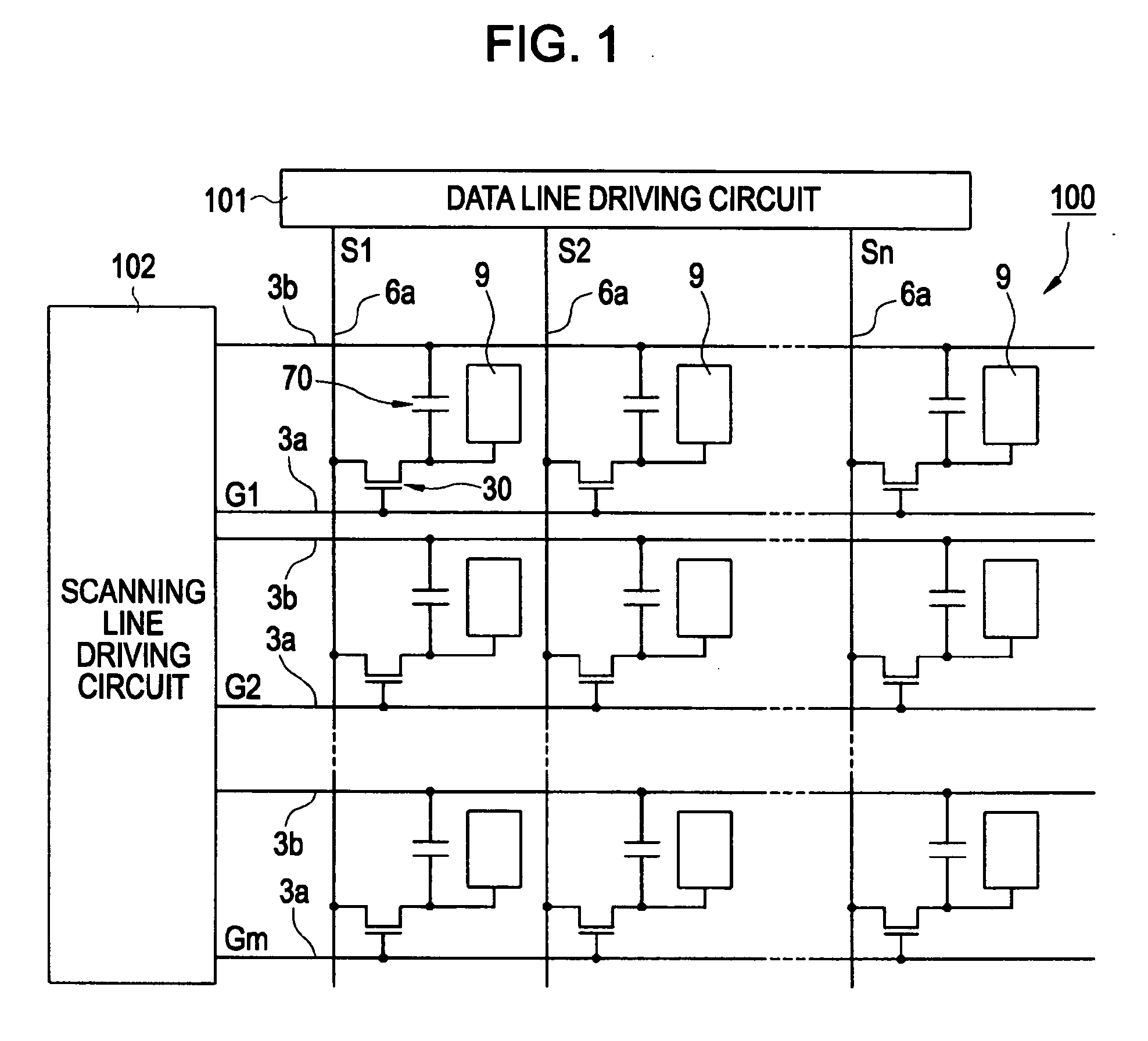
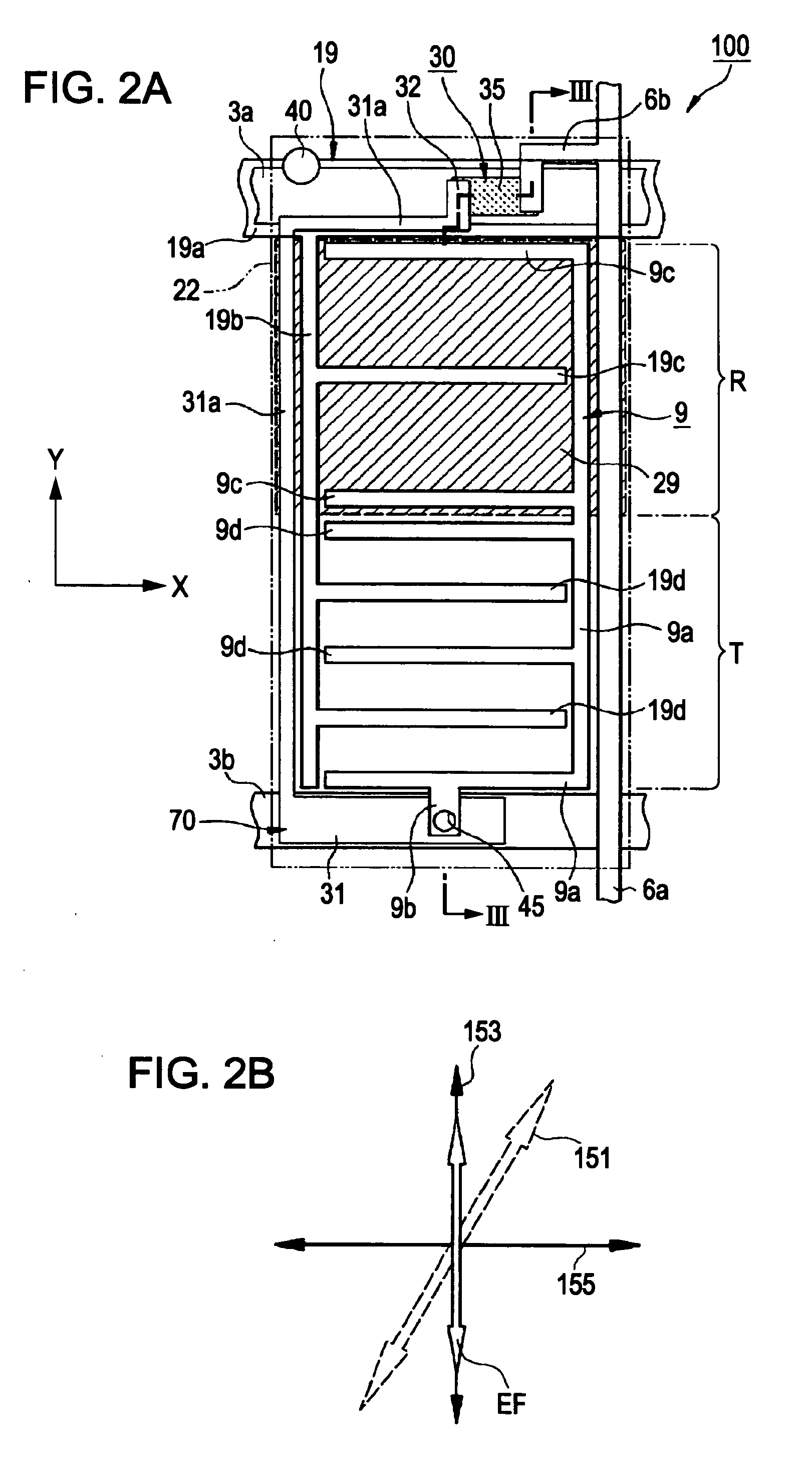
[0030] The liquid crystal device of this embodiment is a color liquid crystal device having color filters on the substrate, and one pixel includes three subpixels which output color light components of R (red), G (green), and B (blue), respectively. Therefore, a display region, which is a minimum unit of display, is referred to as ‘subpixel region’. Further, a...

second embodiment

[0075] Next, a second embodiment of the invention will be described with reference to FIGS. 6 to 8.

[0076]FIG. 6 is a structural plan view showing a certain subpixel region of a liquid crystal device 200 according to this embodiment. FIG. 7 is a partial structural cross-sectional view taken along the line VII-VII of FIG. 6. FIG. 8 is a schematic view showing a part of FIG. 7 for explaining the effects of the liquid crystal device 200.

[0077] The basic configuration of the liquid crystal device 200 according to this embodiment is the same as that of the first embodiment. FIG. 6 corresponds to FIG. 2B in the first embodiment, and FIGS. 7 and 8 correspond to FIGS. 3 and 5 in the first embodiment. Therefore, in FIGS. 6 to 8, the same parts as those of the liquid crystal device 100 in the first embodiment shown in FIGS. 1 to 5 are represented by the same reference numerals and the descriptions thereof will be omitted.

[0078] As shown in FIG. 6, the subpixel region of the liquid crystal d...

third embodiment

[0091] Next, a third embodiment of the invention will be described with reference to FIGS. 9 and 10.

[0092]FIG. 9 is a structural plan view showing a certain subpixel region of a liquid crystal device 300 according to this embodiment. FIG. 10 is a structural cross-sectional view taken along the line X-X of FIG. 9.

[0093] The liquid crystal device 300 of this embodiment is a transverse electric field mode liquid crystal device which performs image display by applying an electric field along the surface of the substrate (transverse electric field) to liquid crystal and performing the alignment control, in particular, an FFS (Fringe Field Switching) mode liquid crystal device. The circuit configuration and the overall configuration of the liquid crystal device 300 of this embodiment is the same as those of the liquid crystal device 100 of the first embodiment. In FIGS. 9 and 10, the same parts as those of the liquid crystal device 100 of the first embodiment shown in FIGS. 1 to 5 are r...


PUM


Abstract

A liquid crystal device includes first and second substrates which are arranged so as to face each other with a liquid crystal layer interposed therebetween, and first and second electrodes which are provided on the first substrate facing the liquid crystal layer. The liquid crystal layer is driven by electric fields generated between the first and second electrodes. A reflective display region for reflective display and a transmissive display region for transmissive display are provided in each of a plurality of subpixel regions. A liquid-crystal-layer-thickness-adjusting layer is provided in at least the reflective display region so as to vary the thickness of the liquid crystal layer in the subpixel region. A gap between the first and second electrodes in a main direction of an electric field in the transmissive display region is narrower than a gap between the first and second electrodes in a main direction of an electric field in the reflective display region.

Description

BACKGROUND [0001] 1. Technical Field [0002] The present invention relates to a liquid crystal device and an electronic apparatus. [0003] 2. Related Art [0004] Examples of known liquid crystal devices include transverse electric field mode liquid crystal devices which can control the alignment of liquid crystal molecules by applying an electric field along the surface of a substrate to a liquid crystal layer. Further, IPS (In-Plane Switching) mode and FFS (Fringe-Field Switching) mode liquid crystal devices with different configurations of the electrodes which generate an electric field to be applied to liquid crystal are known. In recent years, in order to realize a wide viewing angle by means of a transverse electric field system, a transflective liquid crystal device to which the transverse electric field system is applied has been suggested (for example, see JP-A-2003-344837). [0005] The liquid crystal device disclosed in JP-A-2003-344837 is a multi-gap-type liquid crystal device...

Claims


Application Information

Patent Timeline
IPC IPC(8): G09G3/36
CPCG02F1/133555G02F1/134363G09G2300/0456G09G2300/0443G09G3/3648G02F1/1335G02F1/1343
Inventor NISHIMURA, JOJIHIGA, MASAKATSU
Owner JAPAN DISPLAY WEST
Why Eureka
Try Eureka