Liquid crystal display device

a display device and liquid crystal technology, applied in the field of liquid crystal display devices, can solve the problems of deteriorating image display quality and gradual inability to align liquid crystal molecules, and achieve the effect of improving image display quality

Inactive Publication Date: 2006-12-07
JAPAN DISPLAY CENTRAL CO LTD
View PDF6 Cites 39 Cited by
  • Summary
  • Abstract
  • Description
  • Claims
  • Application Information

AI Technical Summary

Benefits of technology

[0011] An object of the present invention is to solve the above-described problems by providing a liquid crystal display device that is capable of improving image display quality.
[0013] In this liquid crystal display device, the transition voltage is alternately set at the first polarity and second polarity, and applied to the liquid crystal display element section. With the application of the transition voltage, it is possible to prevent non-uniform distribution of liquid crystal molecules, which occurs in the initialization for transitioning the alignment state of liquid crystal molecules from the splay alignment to the bend alignment, and to enhance the display quality of images.

Problems solved by technology

If the application of the transition voltage is repeated each time the power is supplied, there arises a problem that liquid crystal molecules gradually become unable to be aligned in a state of the bend alignment completely transitioned from the splay alignment.
Consequently, the image display quality deteriorates due to flicker.

Method used


Image

  • Liquid crystal display device
  • Liquid crystal display device
  • Liquid crystal display device

Examples


first embodiment

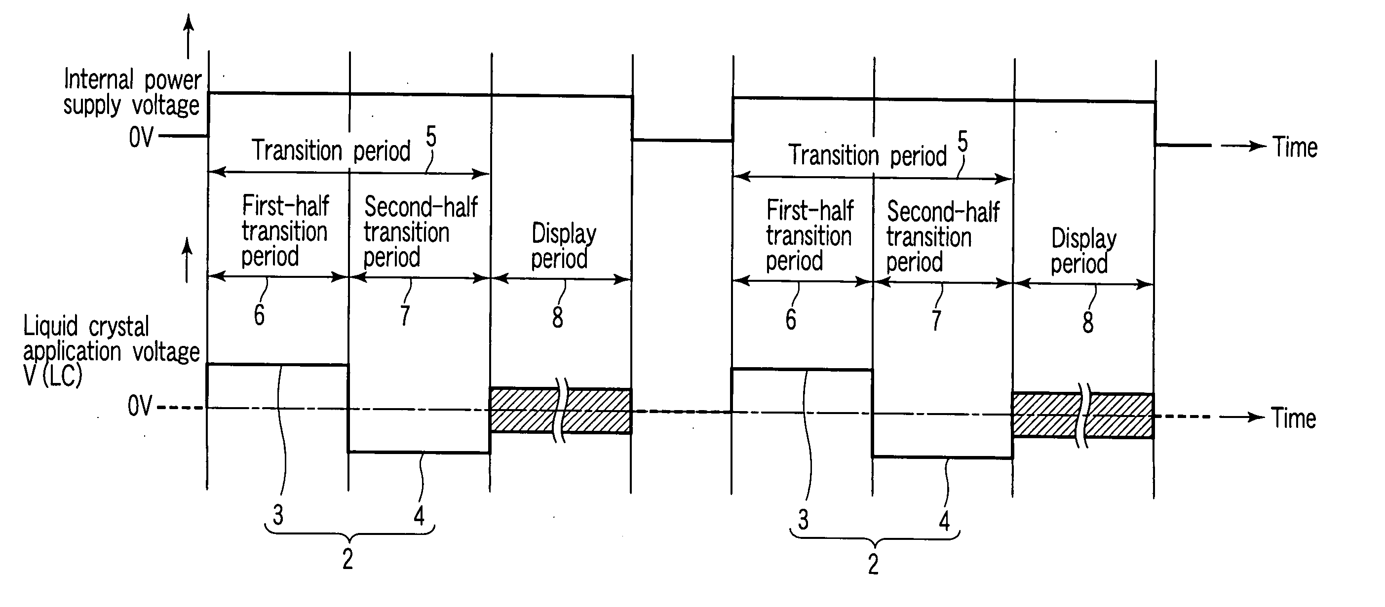
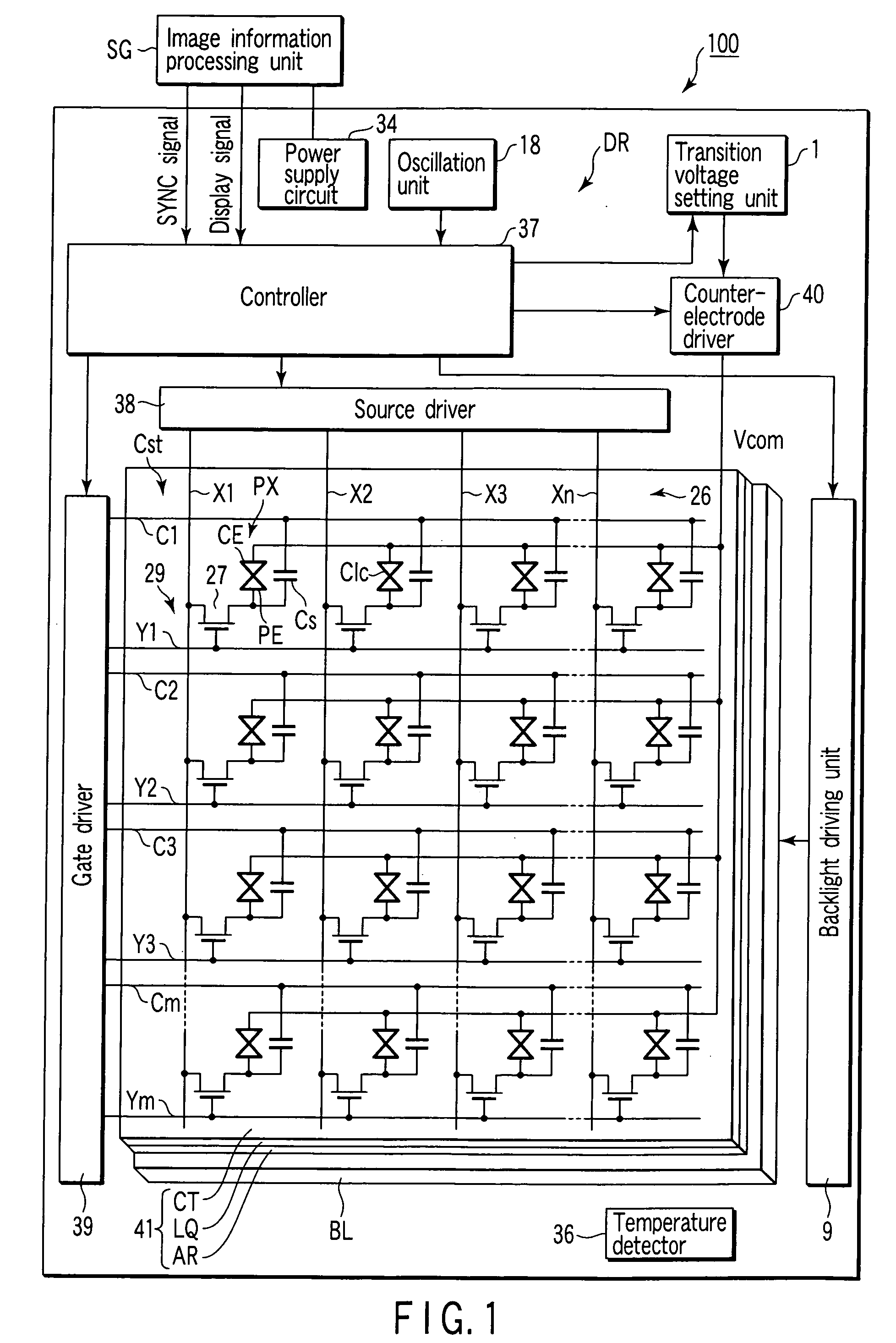
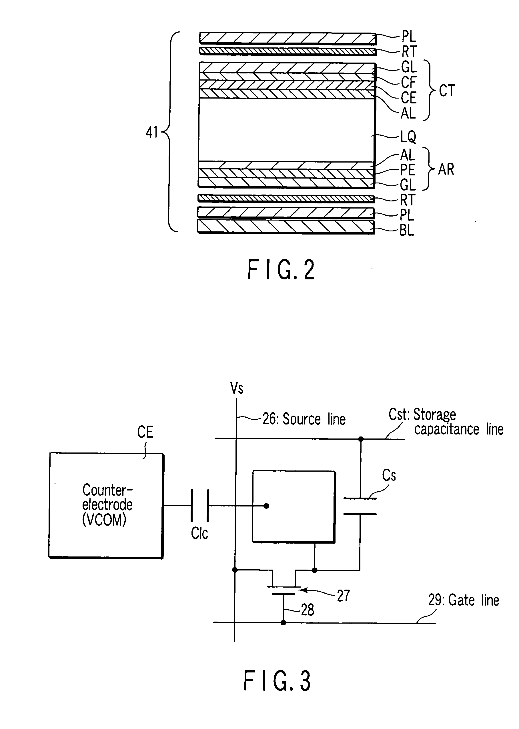
[0051]FIG. 1 schematically shows the circuit configuration of the liquid crystal display device 100, FIG. 2 shows a partial cross-sectional structure of a liquid crystal display (LCD) panel 41 shown in FIG. 1, and FIG. 3 shows the circuit configuration of an OCB liquid crystal display element PX that performs display for one pixel with the cross-sectional structure shown in FIG. 2.

[0052] The liquid crystal display device 100 is connected to an image information process unit SG provided as an external signal source, for example, in a TV set or a mobile phone. The image information processing unit SG performs an image information process to supply a sync signal and a display signal to the liquid crystal display device 100. A power supply voltage for the liquid crystal display device is also supplied from the image information process unit SG to the liquid crystal display device 100.

[0053] The liquid crystal display device 100 includes an LCD panel 41 that provides a matrix array (li...

second embodiment

[0097] A liquid crystal display device according to a second embodiment of the present invention will now be described.

[0098]FIG. 21 shows the configuration of this liquid crystal display device 100A. In FIG. 21, the structural parts common to those in FIG. 1 are denoted by the same reference symbols, and a detailed description is omitted. The liquid crystal display device 100A differs from the device of the first embodiment in that the liquid crystal display device 100A further includes a flicker correction circuit 19, and the counter-electrode driver 40 is replaced with a counter-electrode driver 40A. The flicker correction circuit 19 applies a flicker correction voltage to each OCB liquid crystal display element PX via the counter-electrode driver 40A. This flicker correction voltage is used to correct flicker in an image displayed by the matrix array of OCB liquid crystal display elements PX.

[0099]FIG. 22 shows the configuration of the counter-electrode driver 40A, and FIG. 23...

third embodiment

[0106] A liquid crystal display device according to a third embodiment of the present invention will now be described.

[0107]FIG. 26 shows the configuration of this liquid crystal display device 100B. In FIG. 26, the structural parts common to those in FIG. 21 are denoted by the same reference symbols, and a detailed description is omitted. The liquid crystal display device 100B differs from the device of the second embodiment in that the liquid crystal display device 100B includes a transition voltage polarity memory circuit 35 in place of the oscillation unit 18. The transition voltage polarity memory circuit 35 comprises a nonvolatile memory and stores the polarity of the transition voltage that is applied to the OCB liquid crystal display elements PX.

[0108]FIG. 27 illustrates an operation of the liquid crystal display device 100B. In FIG. 27, the structural parts common to those in FIG. 5 are denoted by the same reference symbols, and a detailed description thereof is omitted. ...


PUM

PropertyMeasurementUnit
reset voltageaaaaaaaaaa
voltageaaaaaaaaaa
temperaturesaaaaaaaaaa

Abstract

A liquid crystal display device includes a liquid crystal display element section that is initialized such that the alignment state of liquid crystal molecules is transitioned from a splay alignment to a bend alignment capable of displaying an image, and a driving circuit that applies, in the initialization, a transition voltage, which causes the alignment state of the liquid crystal molecules to be transitioned from the splay alignment to the bend alignment, to the liquid crystal display element section. In particular, the driving circuit includes a transition voltage setting unit that alternately sets the transition voltage at a first polarity and a second polarity that is opposite to the first polarity.

Description

CROSS-REFERENCE TO RELATED APPLICATIONS [0001] This is a Continuation Application of PCT Application No. PCT / JP2005 / 002652, filed Feb. 18, 2005, which was published under PCT Article 21(2) in Japanese. [0002] This application is based upon and claims the benefit of priority from prior Japanese Patent Application No. 2004-045207, filed Feb. 20, 2004, the entire contents of which are incorporated herein by reference.BACKGROUND OF THE INVENTION [0003] 1. Field of the Invention [0004] The present invention relates to a liquid crystal display device that uses OCB (Optically Compensated Bend) liquid crystal display elements in order to display an image. [0005] 2. Description of the Related Art [0006] The liquid crystal display device includes a liquid crystal display panel that provides a matrix array of OCB liquid crystal display elements. The liquid crystal display panel includes an array substrate in which a plurality of pixel electrodes are covered with an alignment film and arrayed i...

Claims


Application Information

Patent Timeline
Patent Type & Authority Applications(United States)
IPC IPC(8): G09G3/36G02F1/133G02F1/139G09G3/20
CPCG09G3/3648G09G3/3655G09G2320/041G09G2310/063G09G2310/06G09G3/36G09G3/20G02F1/133
Inventor IGARASHI, KAZUAKINAKAO, KENJI
Owner JAPAN DISPLAY CENTRAL CO LTD
Why Eureka
Try Eureka