Reference scheme for a non-volatile semiconductor memory device

a reference scheme and memory device technology, applied in static storage, digital storage, instruments, etc., can solve the problems of multi-bit memory cells and significant reduction of windows

Inactive Publication Date: 2006-12-07
POLARIS INNOVATIONS
View PDF63 Cites 21 Cited by
  • Summary
  • Abstract
  • Description
  • Claims
  • Application Information

AI Technical Summary

Benefits of technology

[0027] An additional advantage of the present invention is that not only array behavior over time of stored information—so-called “retention after-cycling”—is considered but also stress to the cells caused by write cycles. Additionally, environmental conditions such as temperature effects both the reference cells and the memory cells. On the other hand, good reference values are available from the main reference cells. These are not effected by the typical stress to which memory and array reference cells are exposed.
[0028] In a further improved embodiment of the invention, for each wordline an additional status cell is provided. In this status cell, named “Row Guard Reference,” an information is store by a first logical state indicating if one of the memory cells associated to the respective wordline is programmed. Otherwise all memory cells associated to the word line are erased, which is indicated by the other logical state.
[0029] It is a further advantage of embodiments of the present invention that the proposed reference scheme can be applied to all types of volatile memory devices.
[0030] These and other advantages of the present invention will become obvious to those of ordinary skill in the art after reading the following detailed description of the preferred embodiments, which is illustrated in the various figures and drawings.

Problems solved by technology

In multi-level and multi-bit memories, the windows have been significantly reduced and it has become a problem to ensure a correct functionality under all environmental conditions and over the whole life period.
From FIG. 19 it can be seen that in multi-bit memory cells an additional problem arises.

Method used


Image

  • Reference scheme for a non-volatile semiconductor memory device
  • Reference scheme for a non-volatile semiconductor memory device
  • Reference scheme for a non-volatile semiconductor memory device

Examples


Embodiment Construction

[0050] Embodiments of the present invention and embodiments will be described more specifically with reference to the drawings. In the figures, identical or similar components are denoted by identical numerals and their description will not be repeated.

[0051] Non-volatile semiconductor memory devices that are electrically re-writable and erasable are referred to as EEPROMs or NROMs as mentioned previously.

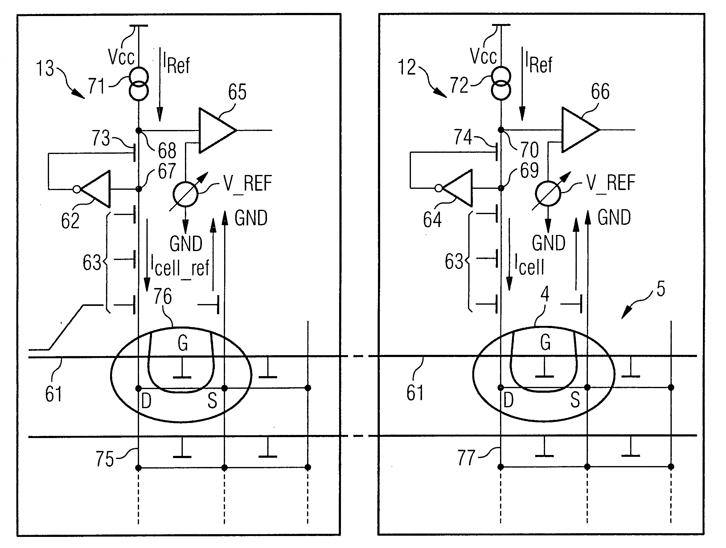
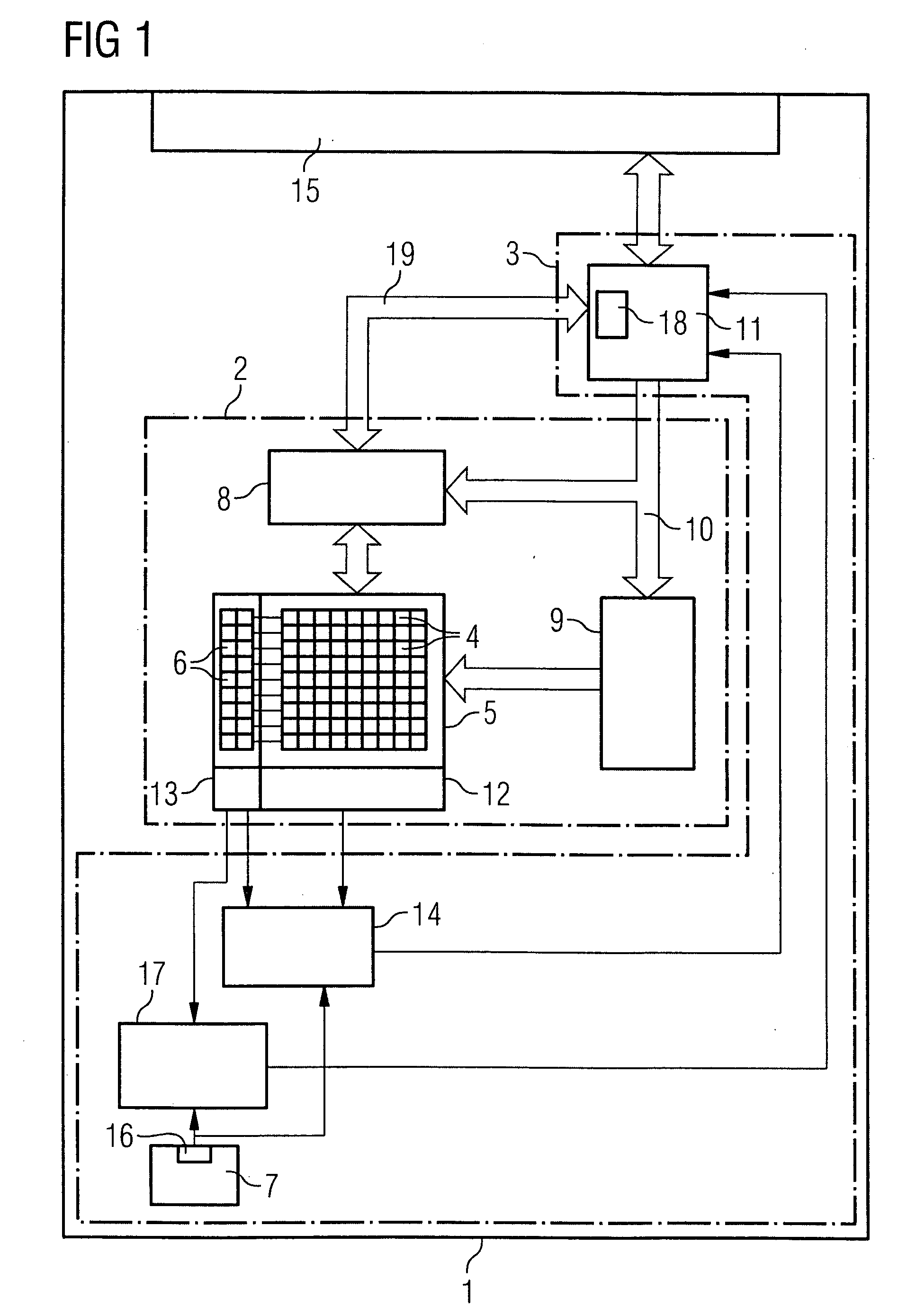
[0052]FIG. 1 is a block diagram showing a configuration of a flash memory device 1 that uses NROM memory cells for storing data. The memory device comprises a memory area 2 and a circuitry area 3. The memory area 2 comprises a memory array 5 with a plurality of memory cells 4. The memory cells are arranged in columns and rows and, therefore, constitute a matrix. Each of the memory cells can be selected by means of a column decoder 8 and a row decoder 9. Both decoders are connected to an address bus 10, which is also connected to a control unit 11 of the circuitry area 3. The cont...


PUM


Abstract

A non-volatile semiconductor memory device is provided comprising a memory area and a circuitry area. The memory area includes a plurality of memory cells and a set of array reference cells that are programmable to have a threshold voltage corresponding to an erased or a programmed state of a memory cell. In the circuitry area, additional main reference cells are provided, which are configured to also have a threshold voltage corresponding to an erased or programmed state of a memory cell. The main reference cells are used for setting of said array reference cells and said array reference cells are provided as a reference for reading or writing a state of said memory cells. A method is also provided for setting array reference cells in a non-volatile semiconductor memory device to a predefined threshold voltage.

Description

TECHNICAL FIELD [0001] The present invention relates to non-volatile semiconductor memory devices. More particularly it relates to a memory device with reference cells that are set up to provide a reference that is adapted to always fit with properties of memory cells, even after a degrade caused by a long operating time or many read or write cycles. The invention also relates to a method for programming reference cells. BACKGROUND [0002] Flash memories have become more and more popular recently, especially in the area of portable communication devices. The basic structure of a flash memory is similar to that of a MOSFET, including a gate, a drain and a source. Usually a flash memory includes a floating gate and a control gate, as the gate of the MOSFET. In addition, there are some kinds of flash memories with no floating gate, such as a nitride read-only memory (NROM). Differing from other types of flash memory that use a conducting polysilicon or metal floating gate, a nitride rea...

Claims


Application Information

Patent Timeline
Patent Type & Authority Applications(United States)
IPC IPC(8): G11C11/34
CPCG11C11/5642G11C16/28G11C16/3418G11C2211/5634G11C16/3436G11C16/349G11C16/3431
Inventor REDAELLI, MARCOAMBROGGI, LUCA DE
Owner POLARIS INNOVATIONS
Why Eureka
Try Eureka