

Process chamber used in manufacture of semiconductor device, capable of reducing contamination by particulates
- Summary
- Abstract
- Description
- Claims
- Application Information
AI Technical Summary
Benefits of technology
Problems solved by technology
Method used
Image

Examples
Embodiment Construction
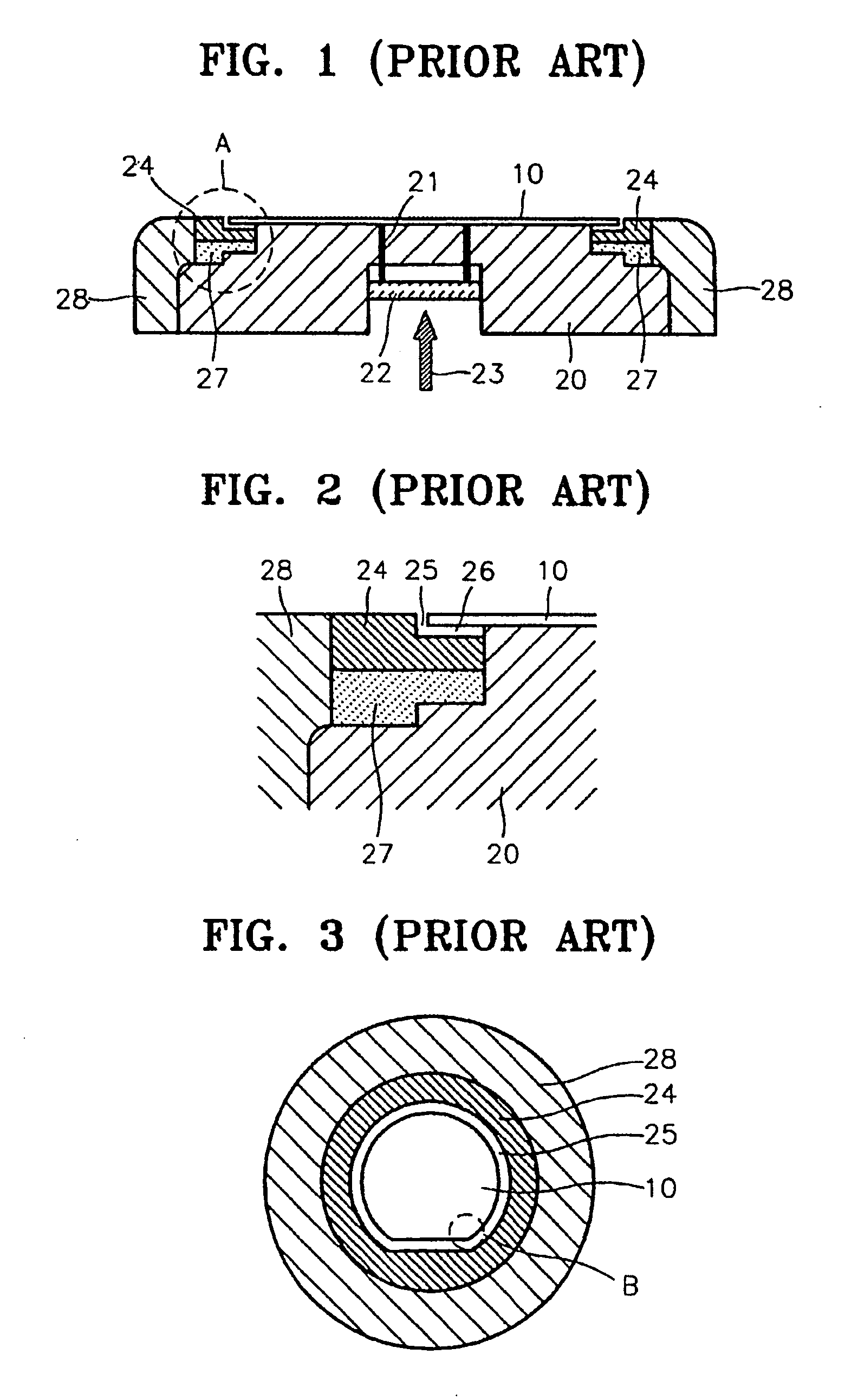
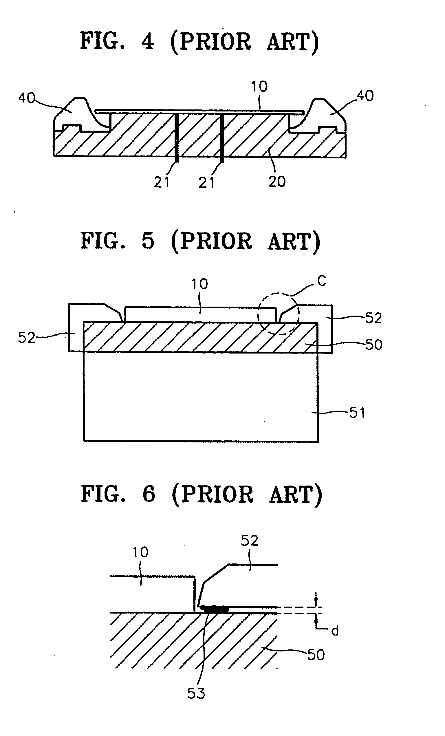
[0047] The present invention now will be described more fully with reference to the accompanying drawings, in which preferred embodiments of the invention are shown. This invention may, however, be embodied in many different forms and should not be construed as being limited to the embodiments set forth herein; rather, these embodiments are provided so that this disclosure will be thorough and complete, and will fully convey the concept of the invention to those skilled in the art. In addition, Korean application nos. 98-39486 and 99-22541, filed Sep. 23, 1998 and Jun. 16, 1999, respectively, are hereby incorporated by reference as if fully set forth herein.
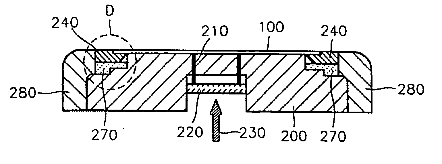
[0048] In accordance with more preferred embodiments of the present invention, the annular edge ring has a first side which faces the side of the semiconductor wafer and contacts the side of the semiconductor wafer. The edge ring preferably has a first upper surface which overlaps the periphery of the bottom surface of the semic...
PUM
| Property | Measurement | Unit |
|---|---|---|
| Thickness | aaaaa | aaaaa |
| Surface temperature | aaaaa | aaaaa |
| Surface temperature | aaaaa | aaaaa |
Abstract
Description
Claims
Application Information