Driving circuit for use with high voltage bidirectional semiconductor switches

a driving circuit and bidirectional semiconductor technology, applied in the direction of pulse technique, process and machine control, instruments, etc., can solve the problem of interruption of the 2deg which turns the switch

Inactive Publication Date: 2006-12-14
INFINEON TECH AMERICAS CORP
View PDF2 Cites 26 Cited by
  • Summary
  • Abstract
  • Description
  • Claims
  • Application Information

AI Technical Summary

Benefits of technology

[0009] A driving circuit for a half bridge utilizing bidirectional semiconductor switches in accordance with an embodiment of the present application includes a high side driver operable to control a high side bidirectional semiconductor switch, wherein the high side driver provides a negative bias voltage to the bidirectional semiconductor switch to turn the high side bidirectional semiconductor switch OFF, a low side driver operable to control a low

Problems solved by technology

The application of an appropriate voltage to either of the gates, ho

Method used


Image

  • Driving circuit for use with high voltage bidirectional semiconductor switches
  • Driving circuit for use with high voltage bidirectional semiconductor switches
  • Driving circuit for use with high voltage bidirectional semiconductor switches

Examples


Embodiment Construction

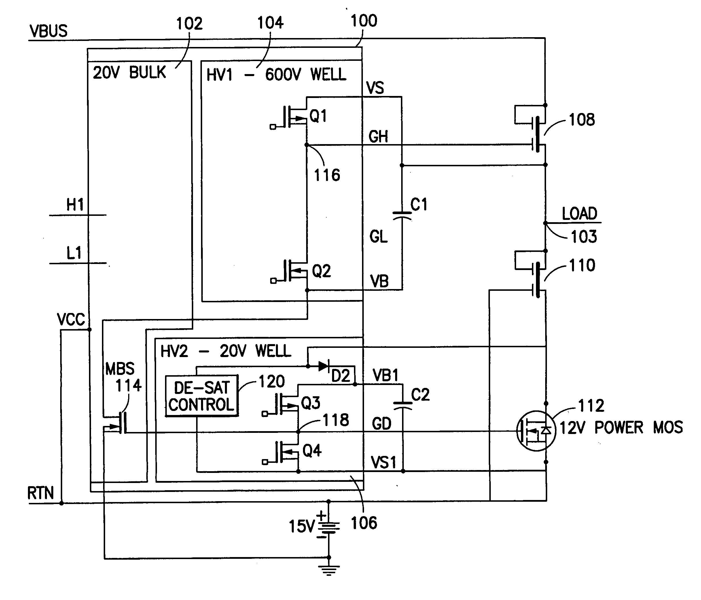
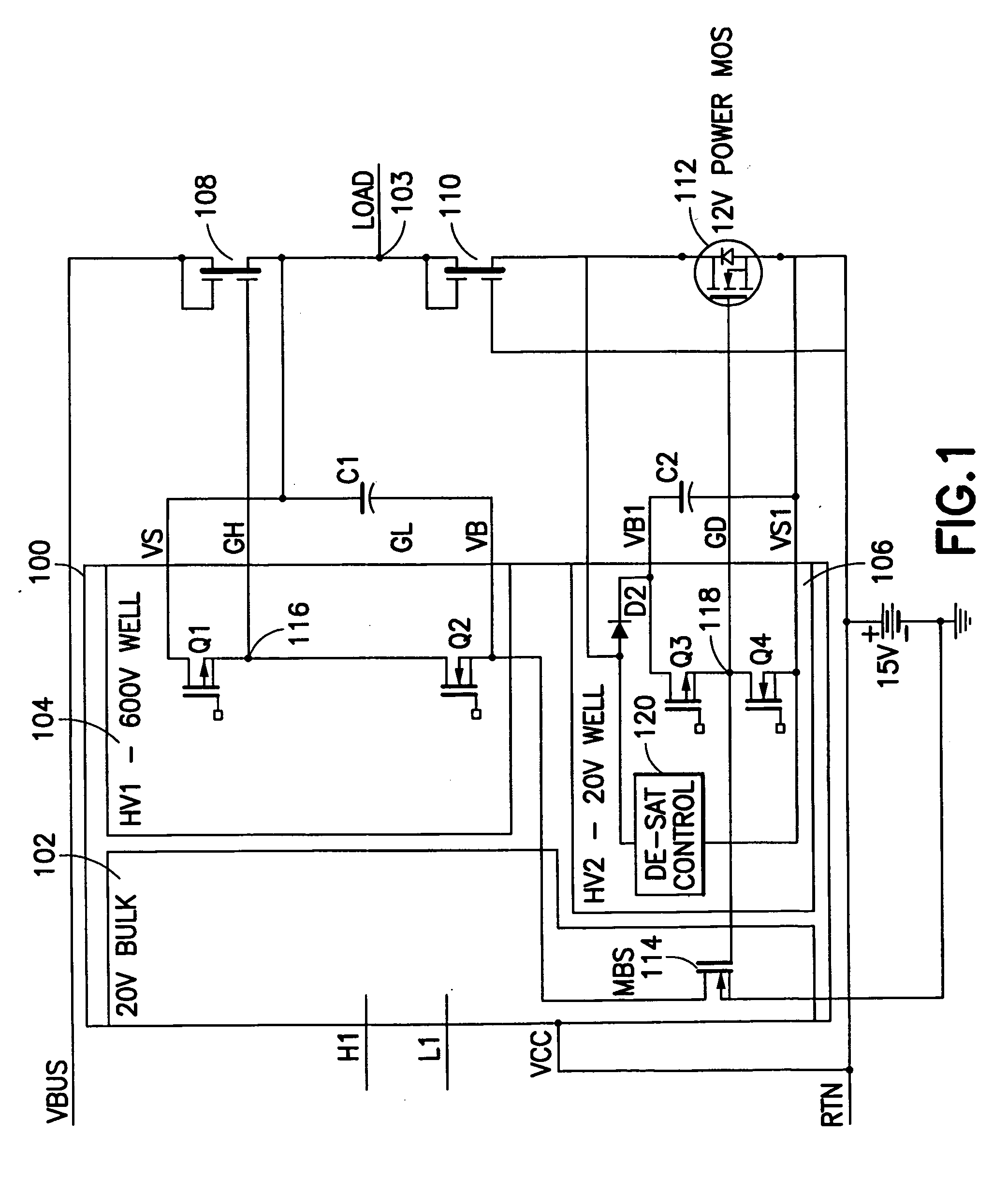
[0021] One of the advantages of using double gated bidirectional semiconductor switches such as those described above, with regard to the topology of accompanying driving circuits is the possibility of having fully equivalent gates each referred to a device source. For example in the specific circuit illustrated in FIG. 1, a gate of a bidirectional semiconductor switching device (108 or 110) is referenced to the positive DC bus rail (VBUS), the negative DC bus rail (RTN) and the half bridge output (node 103).

[0022] Further, given the fact that bidirectional semiconductor switches are depletion mode devices which are normally ON and typically require a negative bias on at least one gate in order to be turned OFF, new driving topologies are possible.

[0023] The circuit of FIG. 1 illustrates a first topology of a driving circuit for a half bridge utilizing bidirectional semiconductor switches 108, 110 in accordance with an embodiment of the present invention.

[0024] As illustrated in ...


PUM


Abstract

A driving circuit for a half bridge utilizing bidirectional semiconductor switches in accordance with an embodiment of the present application includes a high side driver operable to control a high side bidirectional semiconductor switch, wherein the high side driver provides a negative bias voltage to the bidirectional semiconductor switch to turn the high side bidirectional semiconductor switch OFF. A low side driver may be operable to control a low side bidirectional semiconductor switch. An external voltage source with a negative terminal of the voltage source connected to the high side driver may be provided. A high side driving switch may be positioned between the negative terminal of the voltage source and the high side driver and operable to connect the high side driver to the negative terminal of the voltage source when the low side driver turns the low side bidirectional semiconductor switch ON.

Description

CROSS-REFERENCE TO RELATED APPLICATIONS [0001] The present application claims benefit to and priority from U.S. Provisional Patent Application No. 60 / 670,829 entitled DRIVING CIRCUITS AND TECHNIQUES FOR HIGH VOLTAGE, BIDIRECTIONAL SEMICONDUCTOR SWITCHES filed Apr. 13, 2005, the entire contents of which are hereby incorporated by reference herein. [0002] The present application also claims benefit and priority from U.S. Provisional Patent Application No. 60 / 680,629 entitled DRIVING CIRCUIT AND TECHNIQUE FOR HIGH VOLTAGE BIDIRECTIONAL SEMICONDUCTOR SWITCHES filed May 13, 2005, the entire contents of which are hereby incorporated by reference herein.BACKGROUND OF THE INVENTION [0003] 1. Field of the Invention [0004] The present invention relates to driving circuits and methods for use with high voltage bidirectional semiconductor switches. In particular, the present invention provides for a driving circuit that utilizes a bootstrap capacitor and a driving circuit with self supply from ...

Claims


Application Information

Patent Timeline
IPC IPC(8): H03H11/40
CPCH03K17/20H03K17/567H03K2017/6878H03K2017/6875H03K17/6872
Inventor SALATO, MAURIZIOSOLDANO, MARCO
Owner INFINEON TECH AMERICAS CORP
Why Eureka
Try Eureka