Sealed fastenerless multi-board electronic module and method of manufacture

Inactive Publication Date: 2006-12-21
DELPHI TECH INC
18 Cites 12 Cited by

AI-Extracted Technical Summary

Problems solved by technology

While the approach disclosed by Hinze is advantageous because it eliminates the circuit board...

Benefits of technology

[0003] The present invention is directed to a sealed electronic module and manufacturing method including a housing having an open end, a main circuit board and at least one auxiliary circuit board, where the main and auxiliary circuit boards are both secured in the housing without fasteners by a potting material that is applied to the exposed face of the main circuit board. The main circuit board is peripherally supported by a housing ledge, and the auxiliary circuit board is disposed inboard of the main circuit board. A controlled amount of the potting material applied to the exposed face of the main circuit board flows through one or more strategically placed apertures in the...

Abstract

A sealed electronic module includes a housing having an open end, a main circuit board and at least one auxiliary circuit board, where the main and auxiliary circuit boards are both secured in the housing without fasteners by a potting material that is applied to the exposed face of the main circuit board. The main circuit board is peripherally supported by a housing ledge, and the auxiliary circuit board is disposed inboard of the main circuit board. A controlled amount of the potting material applied to the exposed face of the main circuit board flows through one or more strategically placed apertures in the main circuit board, forming one or more bridges of potting material between the main circuit board and the underlying surface of the auxiliary circuit board so that potting material applied in a single step secures both circuit boards in the housing while environmentally sealing the module.

Application Domain

Casings with connectors and PCBPrinted circuit aspects +3

Technology Topic

Manufacturing engineeringMechanical engineering +3

Image

  • Sealed fastenerless multi-board electronic module and method of manufacture
  • Sealed fastenerless multi-board electronic module and method of manufacture
  • Sealed fastenerless multi-board electronic module and method of manufacture

Examples

  • Experimental program(1)

Example

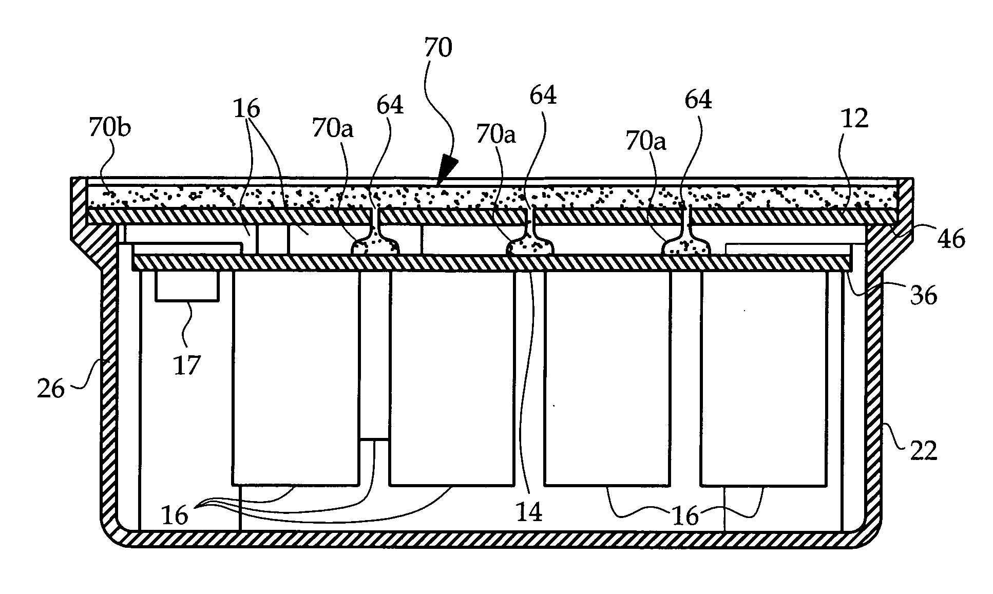
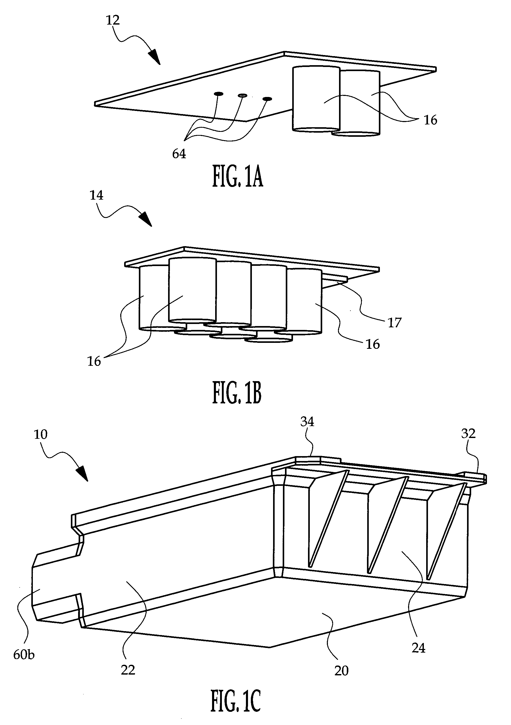
[0010] Referring to FIG. 1, the reference numerals 10, 12 and 14 respectively designate a housing, a main circuit board and an auxiliary circuit board. The main and auxiliary circuit boards 12, 14 are each populated with electronic components such as the capacitors 16 and accelerometer 17, and each board is oriented so that its major components face downward—i.e., toward the bottom 20 of housing 10. In general, the main and auxiliary circuit boards 12, 14 are installed into the housing 10 in the order depicted in FIG. 1, and then sealed in place with a potting material such as polyurethane applied to the exposed face of the main circuit board 12.
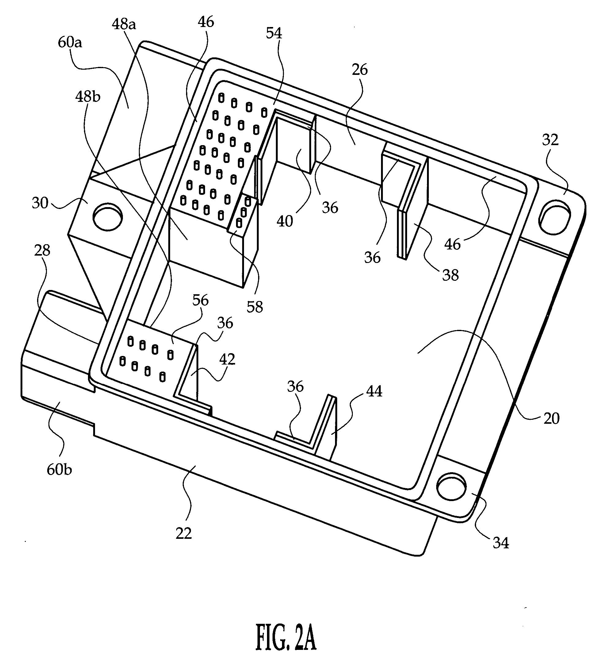
[0011] Referring additionally to FIGS. 2A-2C, the housing 10 includes side walls 22, 24, 26, 28 depending from the bottom 20 and a set of integral mounting tabs 30, 32, 34. The housing 10 is open-ended as shown to receive the populated circuit boards 12, 14. The auxiliary circuit board 14 is installed inboard of the main circuit board 12 as indicated in FIG. 1, and rests on a set of four L-shaped ledges 36 formed by four stepped L-shaped inner housing walls 38, 40, 42, 44 as illustrated in FIGS. 2B and 4. The main circuit board 12 when installed rests on a ledge 46 above the auxiliary circuit board, as illustrated in FIG. 2C. The ledge 46 is formed by a lateral offset in the housing walls 22, 24, 26, 28 and extends around the inner periphery of the housing 10 as shown in FIG. 2A.
[0012] Electrical connections among the main and auxiliary circuit boards 12, 14 and various external devices and circuits are provided by connector pins molded into a pair of connector blocks 48a, 48b. The connector blocks 48a, 48b are preferably insert-molded in the housing 10 and are disposed adjacent the housing wall 28. Referring to FIG. 4, the connector block 48a supports both L-shaped connector pins 50 (only two of which are shown) and J-shaped connector pins 52 (only one of which is shown). Although not illustrated in FIG. 4, the connector pins of connector block 48b are all L-shaped. The L-shaped connector pins 50 of connector blocks 48a, 48b protrude horizontally through the housing wall 28 and vertically through respective connector block surfaces 54, 56 that lie in the same plane as the ledge 46 that supports main circuit board 12. The J-shaped connector pins 52 of connector block 48a protrude vertically through the connector block surface 54 and a connector block surface 58 that lies in the same plane as the ledges 36 that support auxiliary circuit board 14. The terminal portions of the L-shaped connector pins 50 that protrude horizontally through the housing wall 28 are shrouded by connector headers 60a, 60b of housing 10. The terminal portions of the J-shaped connector pins 52 that protrude vertically through the connector block surface 58 electrically interconnect with plated through-holes formed in the auxiliary circuit board 14. And the terminal portions of the L-shaped and J-shaped connector pins 50, 52 that protrude vertically through the connector block surfaces 54, 56 electrically interconnect with plated through-holes formed in the main circuit board 12. Preferably, the terminal portions of the connector pins 50, 52 that protrude vertically through the connector block surfaces 54, 56, 58 are compliant and yield resiliently when passing through the circuit board through-holes so that soldered connections are not required.
[0013] According to the invention, the main and auxiliary circuit boards 12, 14 are both secured the within the housing 10 by the application of a potting material 70 such as polyurethane to the exposed face 62 of main circuit board 12. The potting material 70 is applied in a single step following installation of the main and auxiliary circuit boards 12, 14 as described above. As illustrated in FIGS. 1, 2C and 3, the main circuit board 12 is provided with a set of apertures or through-holes 64 in a portion of the circuit board that overlies the auxiliary circuit board 14. Potting material 70 deposited on the exposed face 62 of the main circuit board 12 floods a volume bounded by the exposed face 62 and portions of the housing side walls 22, 24, 26, 28 that extend above main circuit board 12. When cured, the potting material 70 adheres to the main circuit board 14 and the housing side walls 22, 24, 26, 28 to structurally bond the main circuit board 12 to the housing 10. The potting material 70 is sufficiently thin in its uncured state that it additionally flows into the apertures 64 in the main circuit board 12, forming plugs of cured potting material 70a that bridge the gap between the main and auxiliary circuit boards 12, 14 beneath the apertures 64 as shown in FIG. 3. The potting material plugs 70a structurally bond the auxiliary circuit board 14 to the main circuit board 12 (and hence, to housing 10), and vertically retain the auxiliary circuit board 14 on the ledge 36. Additionally, the layer of cured potting material 70b remaining on the exposed face 62 of main circuit board 12 serves to environmentally seal the module.
[0014] In summary, the present invention provides a sealed electronic module and manufacturing method with fastenerless support of a main circuit board and at least one auxiliary circuit board with a single application of potting material to the exposed face of the main circuit board. While the present invention has been described in reference to the illustrated embodiment, it will be recognized that various modifications will occur to those skilled in the art. For example, the housing 10 may have a shape other than rectangular, there may be more than one auxiliary circuit board, the number of potting material bridges may be different than illustrated, and so forth. Accordingly, it is intended that the invention not be limited to the disclosed embodiment, but that it have the full scope permitted by the language of the following claims.

PUM

no PUM

Description & Claims & Application Information

We can also present the details of the Description, Claims and Application information to help users get a comprehensive understanding of the technical details of the patent, such as background art, summary of invention, brief description of drawings, description of embodiments, and other original content. On the other hand, users can also determine the specific scope of protection of the technology through the list of claims; as well as understand the changes in the life cycle of the technology with the presentation of the patent timeline. Login to view more.
Why Eureka
Try Eureka