III-nitride semiconductor device fabrication

Active Publication Date: 2007-01-04
INFINEON TECH AMERICAS
View PDF46 Cites 14 Cited by
  • Summary
  • Abstract
  • Description
  • Claims
  • Application Information

AI Technical Summary

Benefits of technology

[0007] It is an object of the present invention to reduce the stresses due to material incompatibility in the fabrication of a III-nitride semiconductor device in order to prevent cracking or the like mechani

Problems solved by technology

III-V semiconductors are desirable for power applications, but have not been exploited extensively due in part to difficulties in fabrication.
However, due to lattice mismatch and differences in the thermal expansion characteristics of III-nitride semiconductor alloys and silicon, thick III-nitride semiconductor layers (e.g. more

Method used


Image

  • III-nitride semiconductor device fabrication
  • III-nitride semiconductor device fabrication
  • III-nitride semiconductor device fabrication

Examples


Example

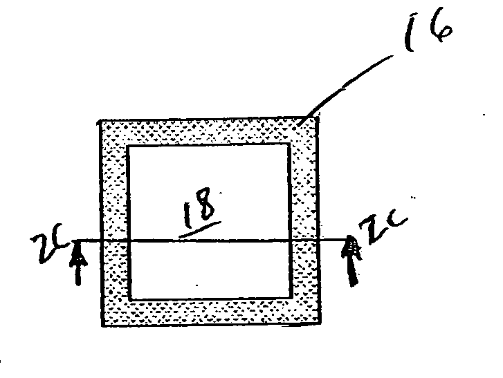
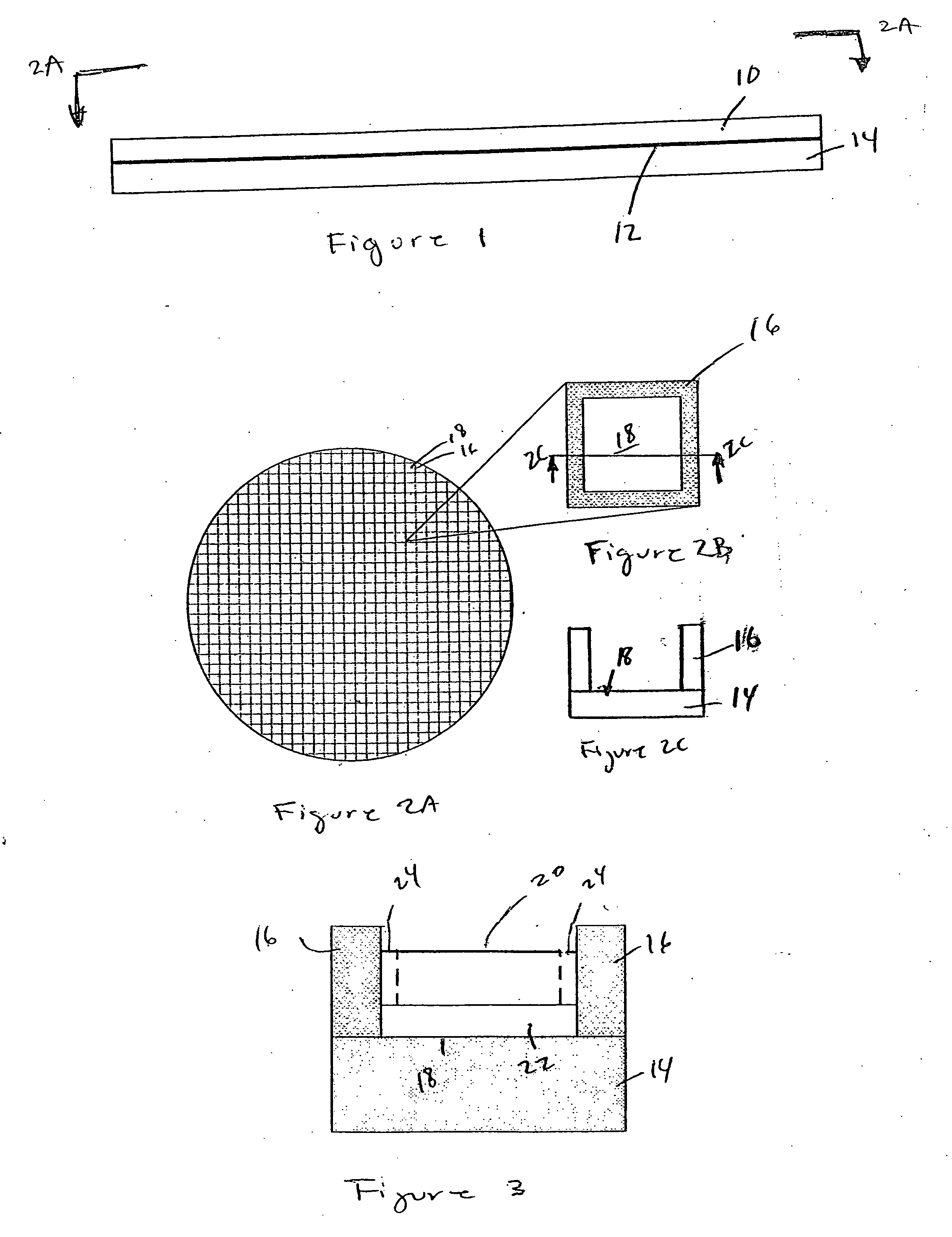
[0026] Referring now to FIG. 3, in a process according to the first embodiment of the present invention, a III-nitride semiconductor body 20 is formed within the space defined by each growth barrier 16 over growth surface 18. Note that III-nitride semiconductor body 20 as referred to herein may include one graded or ungraded III-nitride semiconductor layer, or a plurality of III-nitride semiconductor layers having different compositions. That is, III-nitride semiconductor body 20 as used herein should not be understood to be limited to a single layer of III-nitride semiconductor only.

[0027] Specifically, in the preferred embodiment, an interlayer 22 (or sometimes referred to as buffer layer) is first formed on growth surfaces 18, and then a III-nitride semiconductor body 20 is formed over interlayer 22. It should be noted that the material for forming growth barrier 16 is selected such that it does not allow interlayer 22 and III-nitride semiconductor body 20 to grow on any surface...

Example

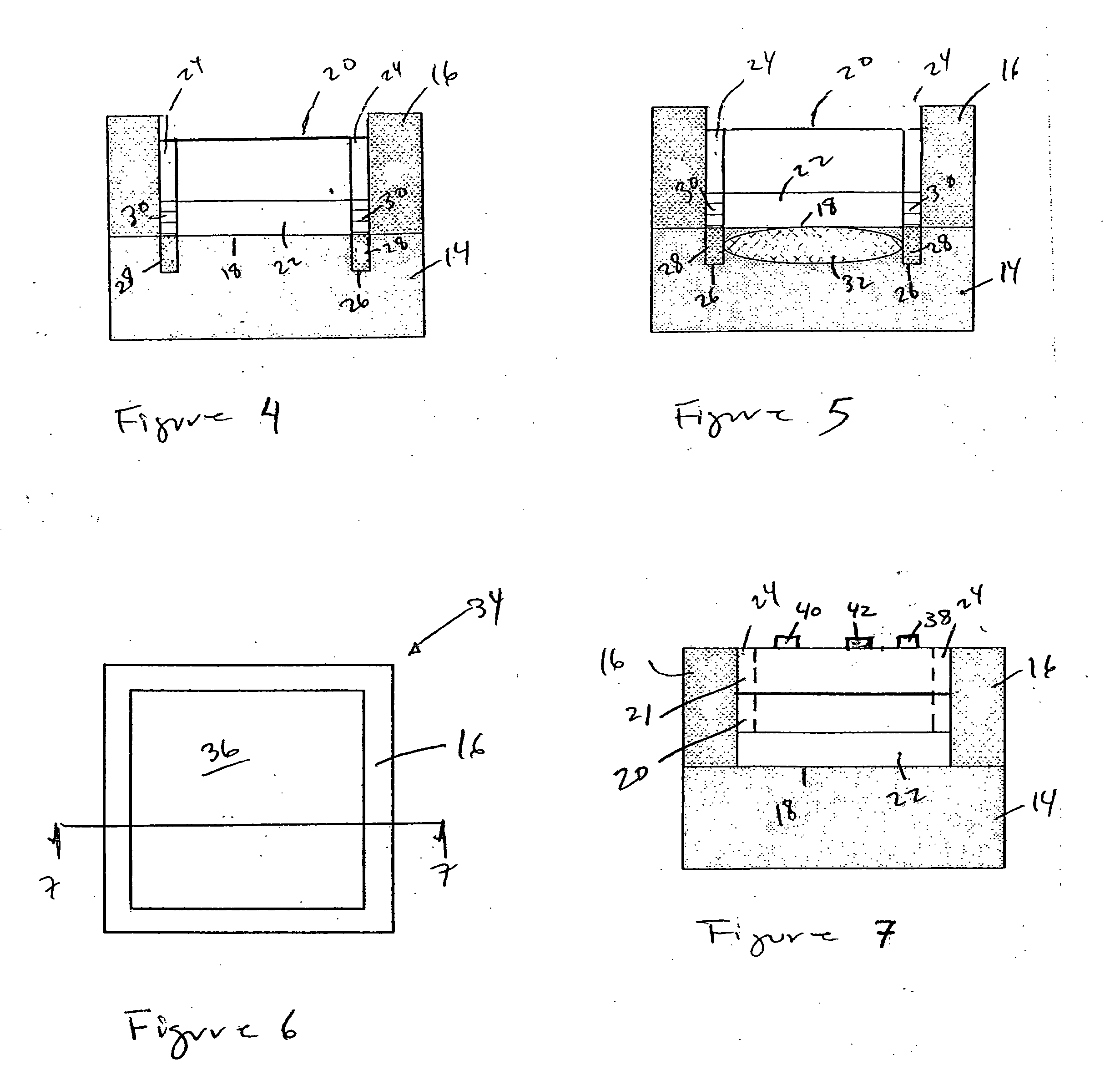
[0031] Referring next to FIG. 5, in a process according to the third embodiment of the present invention the crystal structure of the mesa is damaged by ion implantation or the like in order to form amorphous region 32 therein. Amorphous region 32 can further reduce the stress caused by material incompatibility and thereby prevent cracking of the III-nitride semiconductor body 20. It should be noted that in an alternative process trench 28 can be eliminated and the crystal structure below growth surface 18 can be rendered amorphous in order to obtain the desired stress relief. The remaining steps in a process according to the third embodiment are identical to those in the second or the first embodiment (if trench 28 is omitted), and thus will not be repeated herein for the sake of brevity.

[0032] After forming III-nitride semiconductor body 20, further processing can be carried out as desired to form semiconductor devices such as HEMTs in each cell on substrate 14. Thus, for example...


PUM


Abstract

A method of fabricating a III-nitride power semiconductor device which includes selective prevention of the growth of III-nitride semiconductor bodies to selected areas on a substrate in order to reduce stresses and prevent cracking.

Description

RELATED APPLICATION [0001] This application is based on and claims benefit of U.S. Provisional Application Ser. No. 60 / 690,627, filed Jun. 15, 2005, entitled III-Nitride Semiconductor Device Fabrication, to which a claim of priority is hereby made and the disclosure of which is incorporated by reference.BACKGROUND OF THE INVENTION [0002] The present invention relates to semiconductor devices and more particularly to III-nitride semiconductor devices and methods of fabricating III-nitride semiconductor devices. [0003] A III-V semiconductor is a semiconductor material that is composed of a group III element and a group V element. III-V semiconductors are desirable for power applications, but have not been exploited extensively due in part to difficulties in fabrication. [0004] For example, one commercially desirable III-V semiconductor is III-nitride. Note that as used herein III-nitride semiconductor or GaN-based semiconductor refers to a semiconductor alloy from the InAlGaN system. ...

Claims


Application Information

Patent Timeline
IPC IPC(8): C30B23/00C30B25/00C30B28/12C30B28/14
CPCC30B23/04C30B29/403C30B25/04
Inventor BRIERE, MIKEBEACH, ROBERT
Owner INFINEON TECH AMERICAS
Why Eureka
Try Eureka