Plasma processing method

a processing method and technology of plasma, applied in the direction of decorative surface effects, electrical equipment, decorative arts, etc., can solve the problems of insufficient selective ratio of etching and difficult to use this method for recent miniaturized devices, etc., to achieve sufficient selective ratio, effective removal, and sufficient selective ratio

Inactive Publication Date: 2007-01-04
IKEDA TARO
View PDF9 Cites 2 Cited by
  • Summary
  • Abstract
  • Description
  • Claims
  • Application Information

AI Technical Summary

Benefits of technology

[0008] This invention is developed by focusing the aforementioned problems in order to resolve them effectively. An object of the present invention is to provide a plasma processing method wherein a natural oxide film on a metal or metallic compound film, in particular a CoSi2 film, can be efficiently removed with a sufficient selective ratio.
[0010] According to the present invention, the noble gas and the H2 gas are supplied into the processing container, the plasma is generated in the processing container, and the plasma acts on the natural oxide film formed on a surface of the metal or metallic compound film. Thus, active hydrogen in the plasma reduces the natural oxide film, and active species of the noble gas etch the natural oxide film. As a result, the natural oxide film can be removed with a satisfactory selective ratio.
[0012] It is preferable that the plasma is one of inductive coupling plasma, helicon wave plasma and microwave plasma. Such plasma can be generated independently from a bias-voltage control of a lower electrode for drawing-in the plasma. Thus, the natural oxide film can be removed while less damage is given to the metal or metallic compound film by ions.
[0014] According to the present invention, the noble gas and the H2 gas are supplied into the processing container, the inductive coupling plasma is generated in the processing container, and the plasma acts on the natural oxide film formed on a surface of the CoSi2 film. Thus, active hydrogen in the plasma reduces the natural oxide film, and active species of the noble gas etch the natural oxide film. As a result, the natural oxide film formed on the surface of the CoSi2 film can be removed with a satisfactory selective ratio and without giving any damage by ions to the CoSi2 film. In the case, it is preferable that an etching selective ratio of the natural oxide film with respect to the CoSi2 film is 3 or more.

Problems solved by technology

However, when the natural oxide film on the CoSi2 film is removed by the conventional pre-clean process, the etching selective ratio may not be sufficient.
Thus, it is difficult to use this method for recent miniaturized devices.

Method used


Image

  • Plasma processing method
  • Plasma processing method
  • Plasma processing method

Examples


Embodiment Construction

[0022] Hereinafter, embodiments of the present invention will be described with reference to the attached drawings.

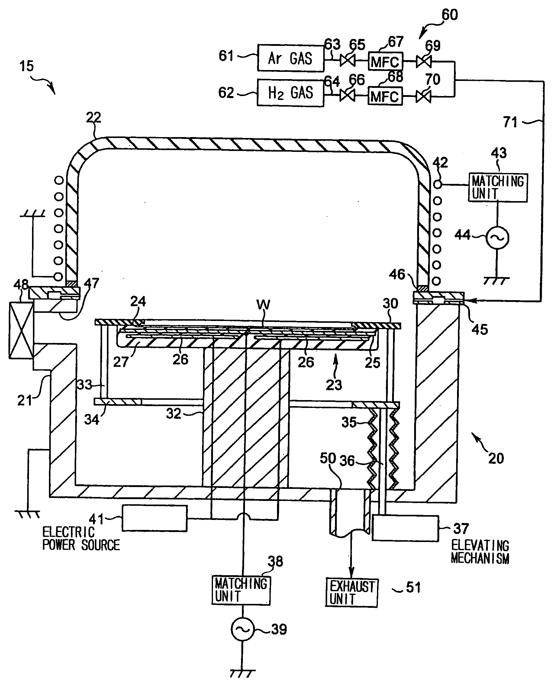
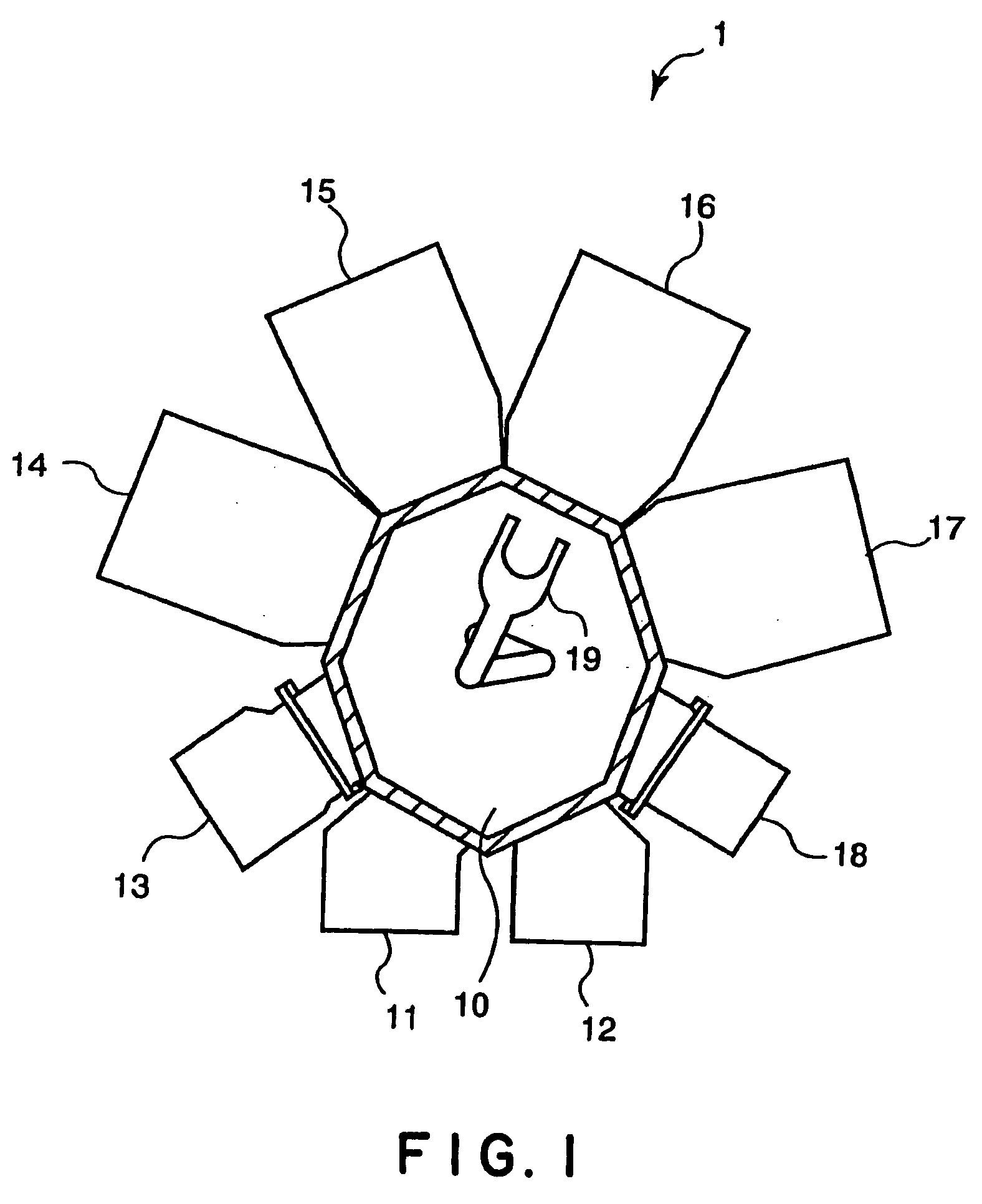
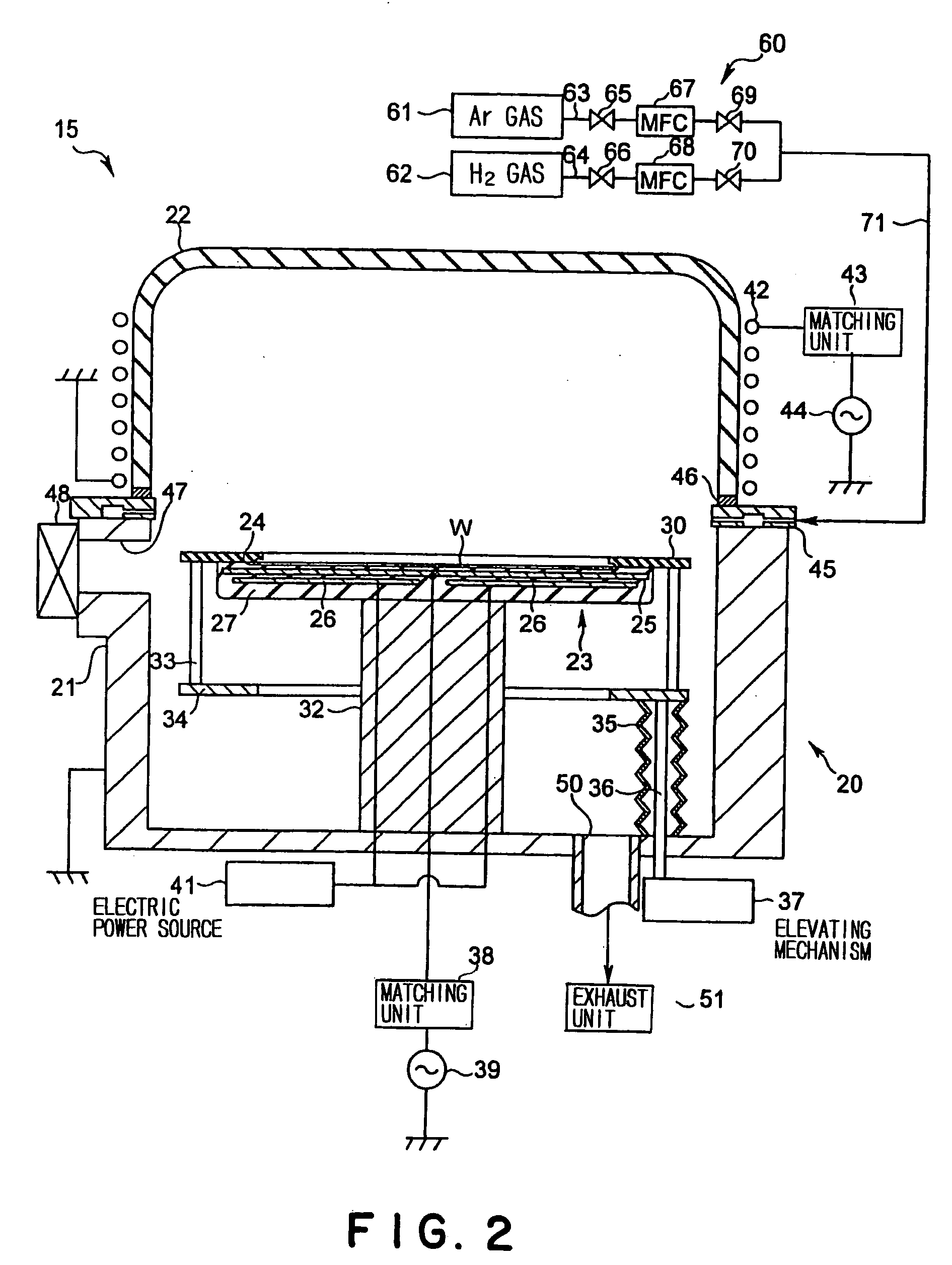
[0023]FIG. 1 is a schematic structural view showing a metal-deposition system including a pre-clean processing unit wherein a plasma processing method according to an embodiment of the present invention is carried out. In the metal-deposition system 1, a transfer chamber 10 is arranged at a central position thereof. Two cassette chambers 11 and 12, a degassing chamber 13, a Ti depositing unit 14, a pre-clean processing unit 15, a TiN depositing unit 16, an Al depositing unit 17 and a cooling chamber 18 are provided around the transfer chamber 10. That is, the metal-deposition system 1 is a multi-chamber type of cluster-tool system.

[0024] In the metal-deposition system 1, a barrier layer is formed on a CoSi2 film on a silicon wafer W (hereinafter, which is referred to as merely a wafer), the silicon wafer W having a contact hole or a via hole, the CoSi2 film being form...


PUM

PropertyMeasurementUnit
frequencyaaaaaaaaaa
frequencyaaaaaaaaaa
pressureaaaaaaaaaa

Abstract

The present invention is a plasma processing method including: a step of introducing a substrate into a processing container, a metal or metallic compound film being formed on a surface of the substrate; a step of supplying a noble gas and an H2 gas into the processing container; and a step of generating plasma in the processing container while the noble gas and the H2 gas are supplied, so that a natural oxide film formed on a surface of the metal or metallic compound film is removed by means of the plasma. According to the invention, the noble gas and the H2 gas are supplied into the processing container, the plasma is generated in the processing container, and the plasma acts on the natural oxide film formed on a surface of the metal or metallic compound film. Thus, active hydrogen in the plasma reduces the natural oxide film, and active species of the noble gas etch the natural oxide film. As a result, the natural oxide film can be removed with a satisfactory selective ratio.

Description

FIELD OF THE INVENTION [0001] The present invention relates to a plasma processing method that is used to remove a natural oxide film formed on a metal film or a metallic compound film, in particular on a CoSi2 film, of a surface of a substrate. DESCRIPTION OF THE RELATED ART [0002] In a semiconductor manufacturing process, a Ti film is deposited on a bottom of a contact hole formed in a silicon wafer as an object to be processed. A barrier layer such as TiN is formed on a TiSi layer, which is formed by interdiffusion of the Ti film and the silicon wafer. In addition, an Al layer, a W layer, a Cu layer or the like is formed on the barrier layer. Thereby, filling of the contact hole and forming of wirings are carried out. Conventionally, a metal-deposition system having a plurality of chambers is used for carrying out the above successive steps. In such a metal-deposition system, in order to obtain good electrical contacts, prior to the deposition process, a process for removing a na...

Claims


Application Information

Patent Timeline
Patent Type & Authority Applications(United States)
IPC IPC(8): C23F1/00H01L21/302H01L21/461C23G5/00H01L21/3065H01L21/768
CPCH01L21/76838C23G5/00H01L21/3065
Inventor IKEDA, TARO
Owner IKEDA TARO
Why Eureka
Try Eureka