TFT and TFT substrate using the same, method of fabricating TFT substrate and liquid crystal display

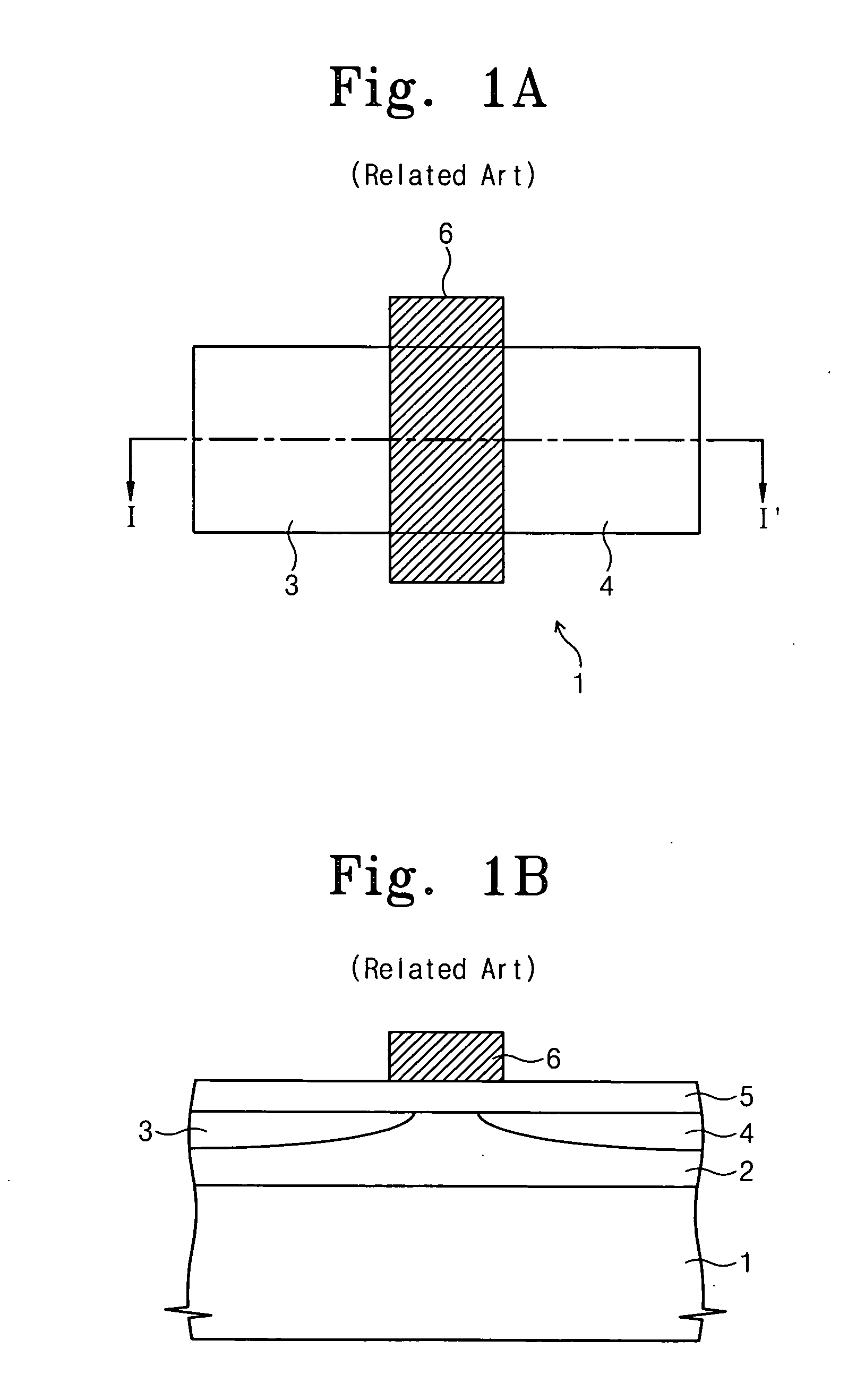
a technology of tft and substrate, which is applied in the direction of instruments, semiconductor devices, optics, etc., can solve the problems of low light sensing capability, electron-hole pairs generated in the source region b>3/b> and the drain region b>4/b> may not have a sufficient energy to pass through the channel region prior to recombination, etc., and achieve the effect of superior light sensing ability

Active Publication Date: 2007-01-18
SAMSUNG DISPLAY CO LTD
View PDF2 Cites 24 Cited by
  • Summary
  • Abstract
  • Description
  • Claims
  • Application Information

AI Technical Summary

Benefits of technology

[0011] Accordingly, embodiments of the present inventio

Problems solved by technology

In addition to the above, the related art TFT has a drawback in that the light sensing capability is low, which will be described in more detail below.
However, the e

Method used


Image

  • TFT and TFT substrate using the same, method of fabricating TFT substrate and liquid crystal display
  • TFT and TFT substrate using the same, method of fabricating TFT substrate and liquid crystal display
  • TFT and TFT substrate using the same, method of fabricating TFT substrate and liquid crystal display

Examples


Embodiment Construction

[0027] The present invention will now be described more fully with reference to the accompanying drawings, in which exemplary embodiments of the invention are shown. The invention may, however, be embodied in many different forms; rather, these embodiments are provided so that this disclosure will be thorough and complete, and will fully convey the concept of the invention to those skilled in the art. Accordingly, the invention should not be construed as being limited to the embodiments set forth herein. In the drawings, the thicknesses of layers and regions are simplified or exaggerated for clarity. Like reference numerals in the drawings denote like elements, and thus their description may be omitted.

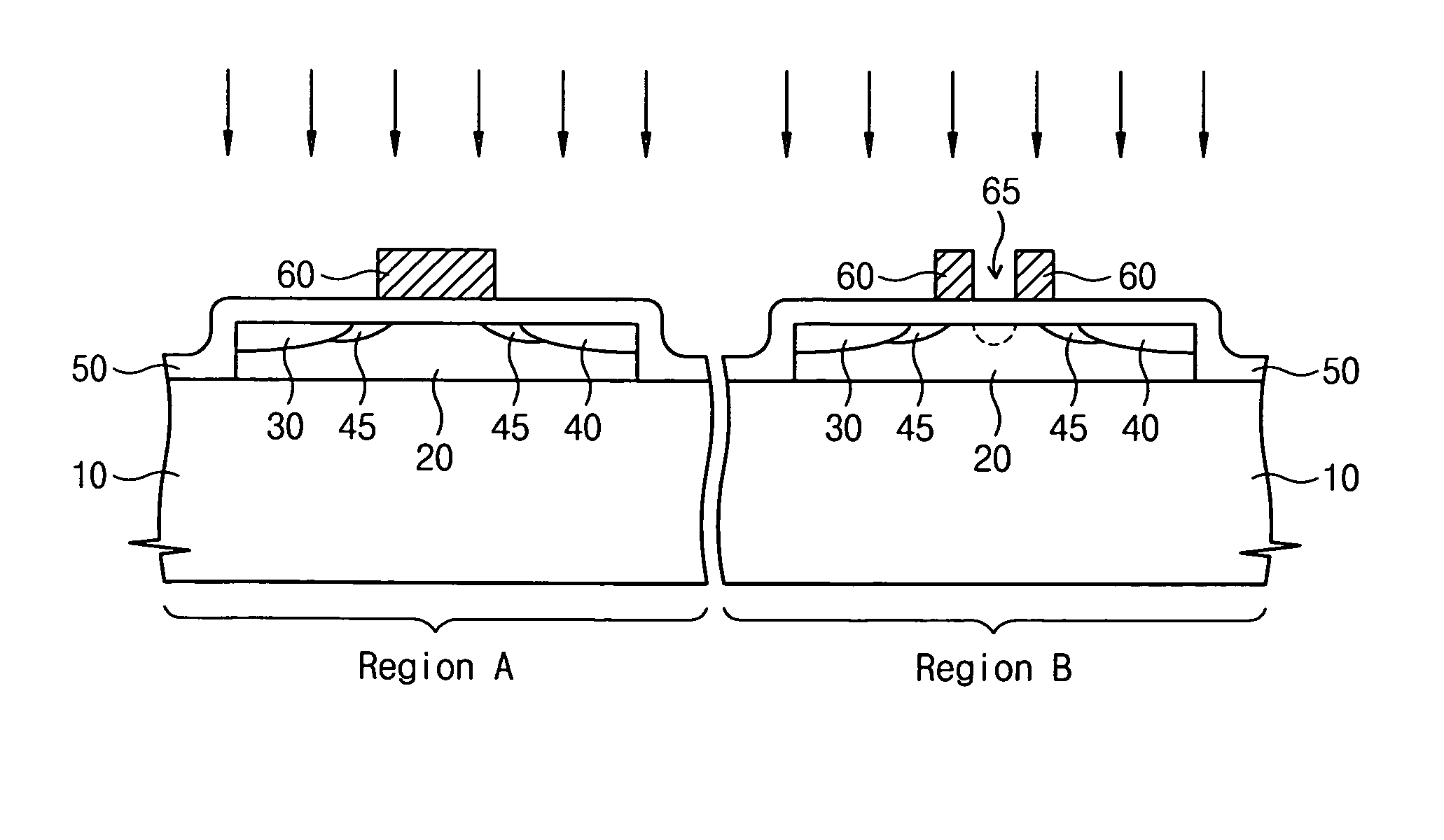
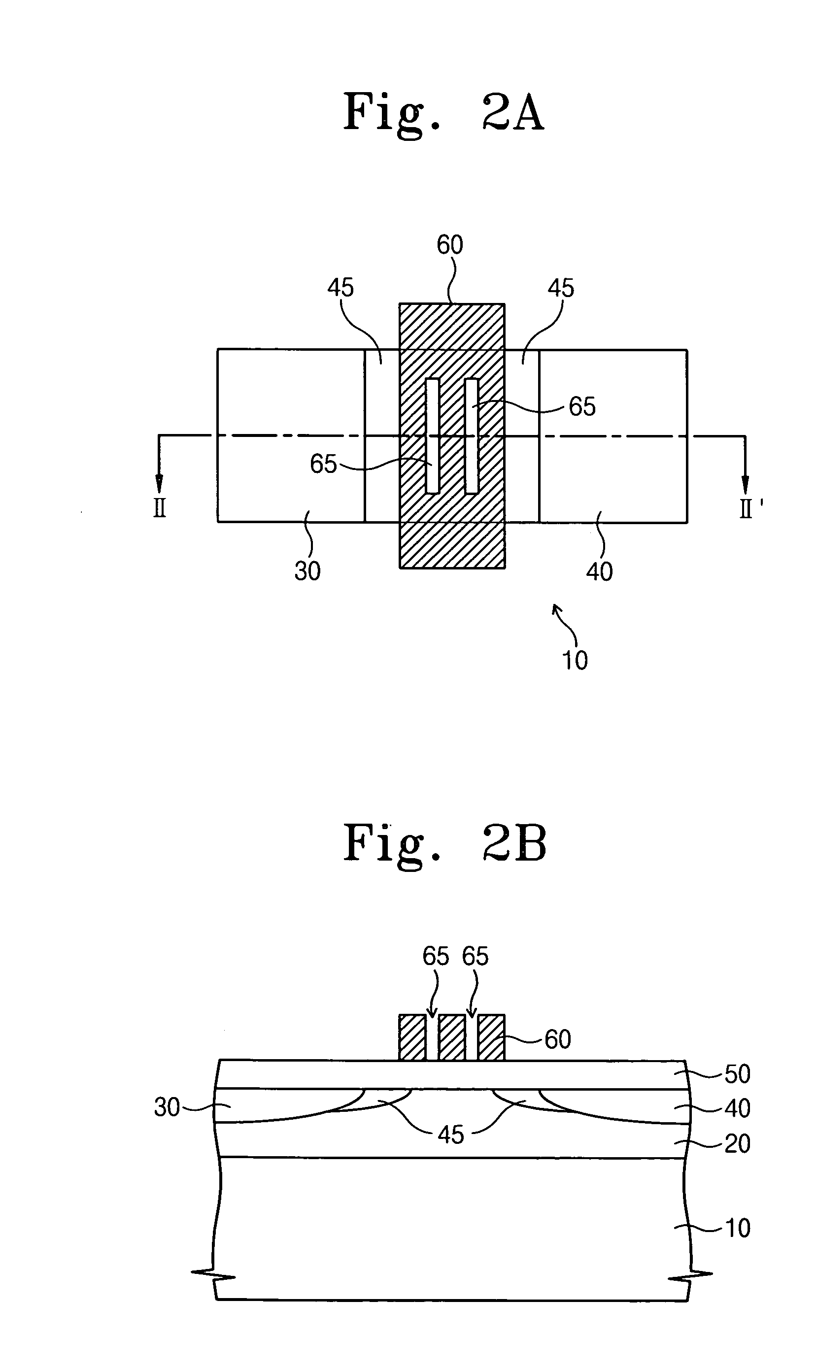
[0028]FIG. 2A is a plane view of a TFT according to an embodiment of the present invention, and FIG. 2B is a sectional view taken along the line of II-II′ of FIG. 2A.

[0029] Referring to FIG. 2A, a gate electrode 60 is formed in a selected direction, and a source region 30 and a drai...


PUM


Abstract

There are provided a TFT, a TFT substrate using the TFT, a method of fabricating the TFT substrate, and an LCD. The TFT includes a source region, a drain region, and a gate electrode having an opening. The opening of the gate electrode is to enhance the light sensing ability of the TFT when it is used as a light sensor, since light is incident into a region where the opening is formed. The TFT including the gate having the opening can be used in a substrate of a flat display or an LCD using such a substrate. The above TFT can sense light incident from outside the display to adjust the brightness of the screen according to the external illumination.

Description

CROSS REFERENCE TO RELATED APPLICATIONS [0001] This application claims priority to Korean Patent application number 2005-63870, filed on Jul. 14, 2005, which is hereby incorporated by reference in its entirety. BACKGROUND OF THE INVENTION [0002] 1. Field of the Invention [0003] The present invention relates to a TFT and an LCD using the same, and more particularly, to a TFT usable as a light sensor, a TFT substrate using the TFT, a method of fabricating the TFT substrate and an LCD. [0004] 2. Description of the Related Art [0005] In general, flat panel displays are one type of display having a slim profile and providing a flat picture. Flat panel displays include liquid crystal displays (LCDs), which are widely used as notebook computer monitors, organic electroluminescent devices (OELDs), which are widely used in cellular phones, etc. In such flat panel displays, thin film transistors (TFTs) are generally used as switching elements for independently operating the respective pixels....

Claims


Application Information

Patent Timeline
IPC IPC(8): G02F1/136
CPCG02F1/13318G02F1/133308G02F2001/13332H01L29/78621H01L27/1214H01L29/42384G02F2201/58G02F1/13332H01L27/124G02F1/136
Inventor JUNG, KWAN-WOOKKIM, UNG-SIKCHOI, PIL-MOSONG, SEOCK-CHEONMAENG, HO-SUKLEE, SANG-HOONPARK, KEUN-WOO
Owner SAMSUNG DISPLAY CO LTD
Why Eureka
Try Eureka