

Imaging lens assembly
a technology of imaging lens and assembly, which is applied in the field of imaging lens assembly, can solve the problems of difficult manufacturing, complicated process of making glass lens adhered together, and inability to reduce the total track length of the system, so as to achieve the effect of reducing the size, reducing the total track length of the imaging lens assembly, and high resolution
- Summary
- Abstract
- Description
- Claims
- Application Information
AI Technical Summary
Benefits of technology
Problems solved by technology
Method used
Image

Examples
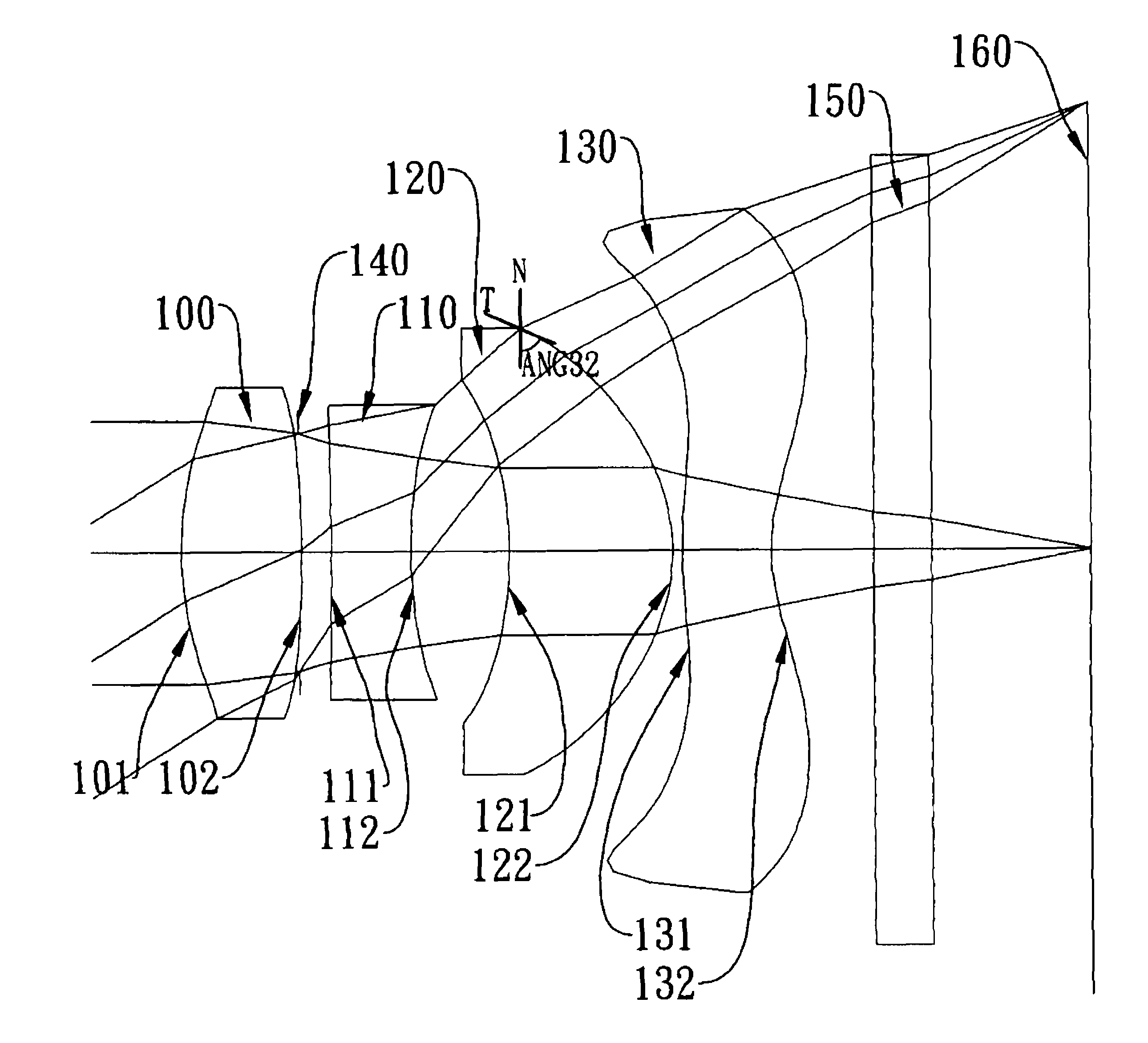
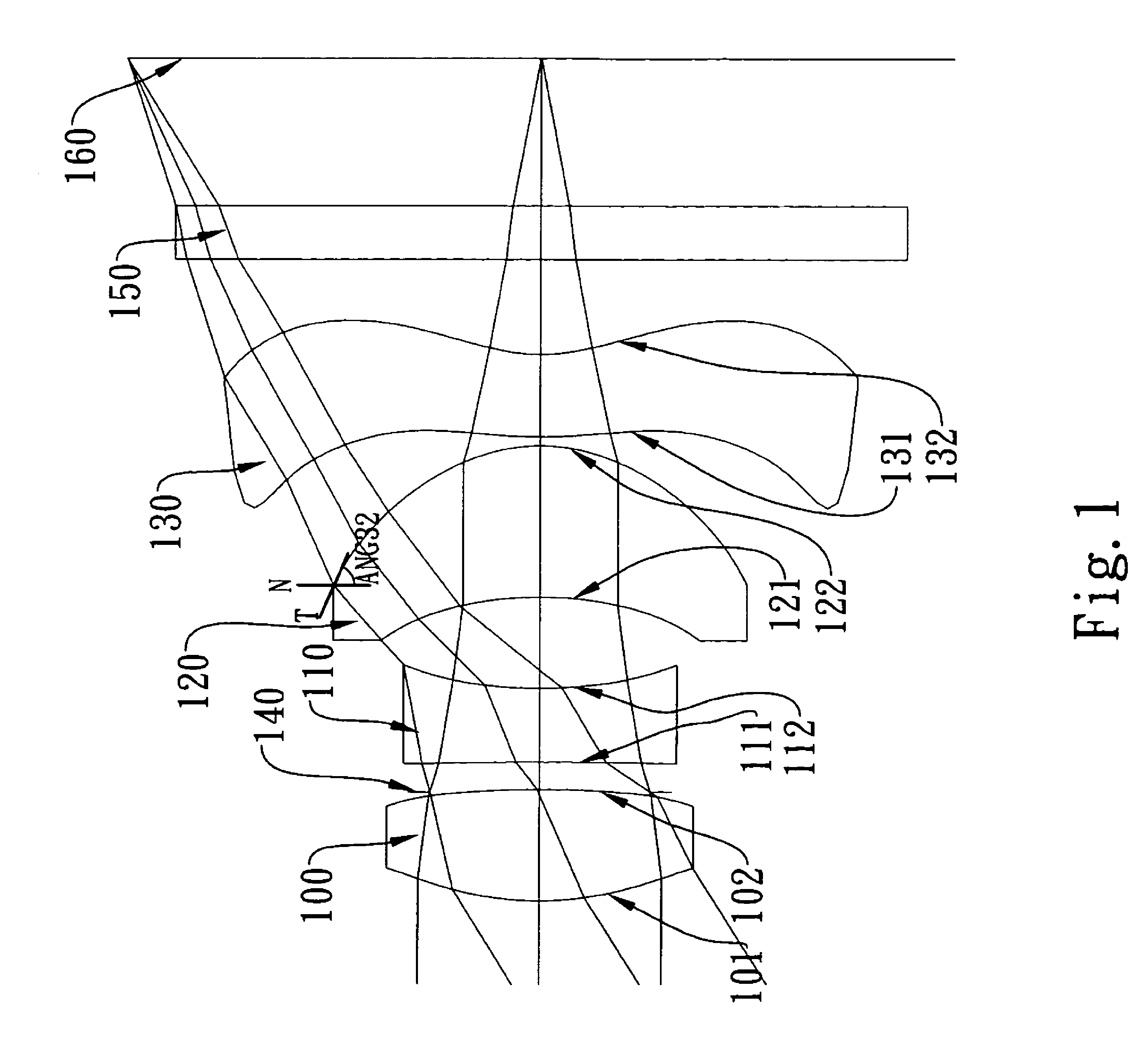
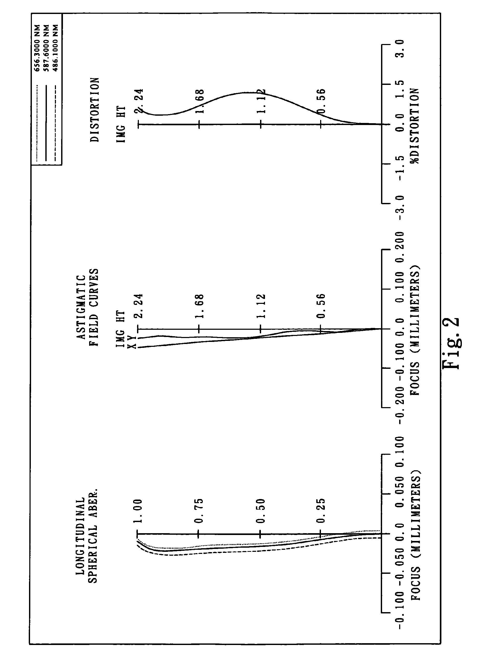
first embodiment
[0069]In the present imaging lens assembly, the focal length of the imaging lens assembly is f, and it satisfies the relation: f=3.68 (mm).
[0070]In the first embodiment of the present imaging lens assembly, the f-number of the imaging lens assembly is Fno, and it satisfies the relation: Fno=2.80.
[0071]In the first embodiment of the present imaging lens assembly, half of the maximal field of view of the imaging lens assembly is HFOV, and it satisfies the relation: HFOV=31.2 deg.
[0072]In the first embodiment of the present imaging lens assembly, the on-axis spacing between the aperture stop 140 and the electronic sensor is SL, the on-axis spacing between the object-side surface 101 of the first lens element 100 and the electronic sensor is TTL, and they satisfy the relation: SL / TTL=0.82.
[0073]In the first embodiment of the present imaging lens assembly, the focal length of the imaging lens assembly is f, the focal length of the first lens element 100 is f1, and they satisfy the relati...
second embodiment
[0086]In the present imaging lens assembly, the focal length of the imaging lens assembly is f, and it satisfies the relation: f=3.53 (mm).
[0087]In the second embodiment of the present imaging lens assembly, the f-number of the imaging lens assembly is Fno, and it satisfies the relation: Fno=2.80.
[0088]In the second embodiment of the present imaging lens assembly, half of the maximal field of view of the imaging lens assembly is HFOV, and it satisfies the relation: HFOV=32.0 deg.
[0089]In the second embodiment of the present imaging lens assembly, the on-axis spacing between the aperture stop 340 and the electronic sensor is SL, the on-axis spacing between the object-side surface 301 of the first lens element 300 and the electronic sensor is TTL, and they satisfy the relation: SL / TTL=0.82.
[0090]In the second embodiment of the present imaging lens assembly, the focal length of the imaging lens assembly is f, the focal length of the first lens element 300 is f1, and they satisfy the re...
third embodiment
[0103]In the present imaging lens assembly, the focal length of the imaging lens assembly is f, and it satisfies the relation: f=3.82 (mm).
[0104]In the third embodiment of the present imaging lens assembly, the f-number of the imaging lens assembly is Fno, and it satisfies the relation: Fno=2.85.
[0105]In the third embodiment of the present imaging lens assembly, half of the maximal field of view of the imaging lens assembly is HFOV, and it satisfies the relation: HFOV=30.1 deg.
[0106]In the third embodiment of the present imaging lens assembly, the on-axis spacing between the aperture stop 540 and the electronic sensor is SL, the on-axis spacing between the object-side surface 501 of the first lens element 500 and the electronic sensor is TTL, and they satisfy the relation: SL / TTL=0.80.
[0107]In the third embodiment of the present imaging lens assembly, the focal length of the imaging lens assembly is f, the focal length of the first lens element 500 is f1, and they satisfy the relati...
PUM
 Abstract
Description
Claims
Application Information