Complementary metal oxide semiconductor image sensor and method for fabricating the same

a metal oxide semiconductor and image sensor technology, applied in the field of complementary metal oxide semiconductor (cmos) image sensors, can solve the problems of small photosensitivity of cmos image sensors, inability to sufficiently generate carriers for floating diffusion, and inability to adequately generate the absorption coefficient of crystalline silicon for visible rays of 1.1 m or less. to achieve the effect of increasing the photosensitivity

Active Publication Date: 2007-07-05
KOREA ADVANCED INST OF SCI & TECH
View PDF4 Cites 56 Cited by
  • Summary
  • Abstract
  • Description
  • Claims
  • Application Information

AI Technical Summary

Benefits of technology

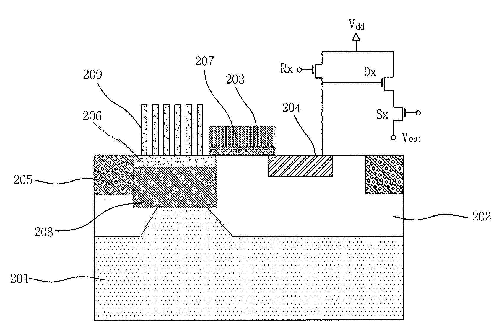
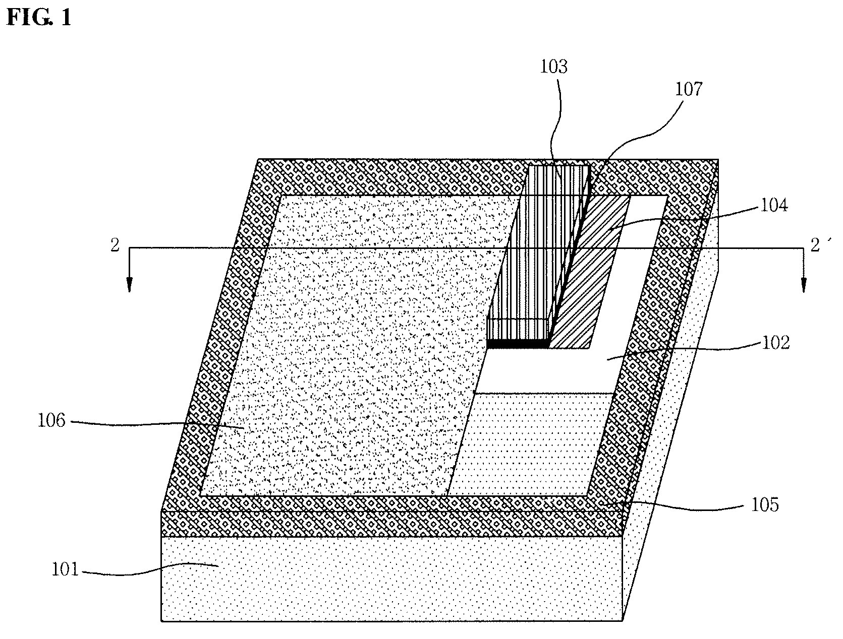
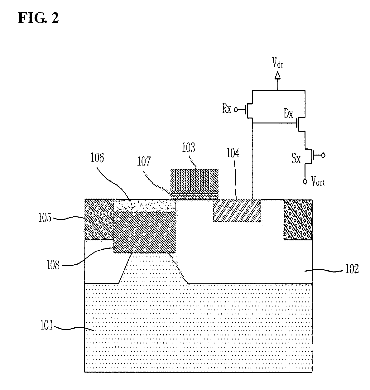
[0020]Accordingly, the present invention is to provide a CMOS image sensor of a new structure, for increasing a photosensitivity even in case where the CMOS image sensor is high integrated.

Problems solved by technology

However, despite having the lower power and the high integration, the CMOS image sensor has a disadvantage that it has a smaller photosensitivity than the conventional CCD image sensor due to a dark current.
However, the absorption coefficient of the crystalline silicon for the visible rays of the wavelength of 1.1 μm or less cannot sufficiently generate carriers transferred to the floating diffusion 104.
Thus, in the crystalline silicon of the light receiving portion, its absorption coefficient is too small to sufficiently form the carriers.
Second, there is a loss of light not absorbed but reflected from the crystalline silicon that is the light receiving portion.

Method used


Image

  • Complementary metal oxide semiconductor image sensor and method for fabricating the same
  • Complementary metal oxide semiconductor image sensor and method for fabricating the same
  • Complementary metal oxide semiconductor image sensor and method for fabricating the same

Examples


first embodiment

[0063]FIG. 5 is a sequential diagram illustrating a method for fabricating a CMOS image sensor according to an exemplary embodiment of the present invention. In FIG. 5, (a) is a diagram illustrating a process of injecting a plasma gas into a light receiving region, (b) is a diagram illustrating nanodusts formed after the injection of the plasma gas, (c) is a diagram illustrating a process of forming nanopillars after a plasma discharge.

[0064]FIG. 6 is a photograph taken by a scanning electron microscopy (SEM), for illustrating the CMOS image sensor fabricated by the method of FIG. 5.

[0065]The method for fabricating the CMOS image sensor according to the first exemplary embodiment of the present invention employs a plasma discharge and etching process, not a conventional photolithography process, to form the nanopillars. It is a method for making polymer components generated in plasma etching into the nanodusts, and using the nanodusts as a mask for forming the nanopillars.

[0066]As f...

second embodiment

[0071]FIG. 7 is a sequential diagram illustrating a method for fabricating a CMOS image sensor according to another exemplary embodiment of the present invention. In FIG. 7, (a) is a diagram illustrating a process of forming a sphere ball in a light receiving region, (b) is a diagram illustrating an etching process using the sphere ball as a mask, (c) is a diagram illustrating a light receiving element after the etching process.

[0072]FIG. 8 is a photograph taken by a SEM, for illustrating the CMOS image sensor fabricated by the method of FIG. 7.

[0073]According to a second exemplary embodiment of the present invention, the method for fabricating the CMOS image sensor employs a nanosphere lithography method to form a nanopillar, and has an advantage of forming the nanopillar beyond a limitation of a resolution of a conventional photolithography method.

[0074]Referring first to (a) of FIG. 7, a photoresist 402 is formed on a silicon substrate 401, and the sphere balls 403 having sizes o...


PUM


Abstract

Provided are a CMOS image sensor and a method for fabricating the same. A nanopillar is plurally formed at an upper end of a light receiving element.

Description

[0001]This Nonprovisional application claims priority under 35 U.S.C. § 119(a) on Patent Application No. 10-2006-0001335 filed in Korea on Jan. 5, 2006, the entire contents of which are hereby incorporated by reference.BACKGROUND[0002]1. Field[0003]The present invention relates to a complementary metal oxide semiconductor (CMOS) image sensor, and more particularly, to a CMOS image sensor having a great photosensitivity and a method for fabricating the same.[0004]2. Description of the Background Art[0005]A charge-coupled device (CCD) image sensor has been much used owing to its simple circuit and its good performance about a picture quality and a noise. However, because a mobile equipment needs a low power and a high integration, attention is being paid to a complementary metal oxide semiconductor (CMOS) image sensor satisfying the low power and the high integration.[0006]The CMOS image sensor refers to a semiconductor device for converting an optical image into an electric signal. T...

Claims


Application Information

Patent Timeline
Patent Type & Authority Applications(United States)
IPC IPC(8): H01L31/113H01L21/00
CPCH01L27/14603H01L27/1462H01L27/14689H01L27/14685H01L27/14643Y10S977/762Y10S977/814Y10S977/954A47G1/02A47G25/28
Inventor CHOI, YANG-KYUKIM, KUK-HWAN
Owner KOREA ADVANCED INST OF SCI & TECH
Why Eureka
Try Eureka