Semiconductor memories with block-dedicated programmable latency register

a programmable latency register and memory device technology, applied in the direction of information storage, static storage, digital storage, etc., can solve the problem that the memory device's total memory performance will experience critical losses

Active Publication Date: 2007-01-25
SAMSUNG ELECTRONICS CO LTD
View PDF8 Cites 131 Cited by
  • Summary
  • Abstract
  • Description
  • Claims
  • Application Information

AI Technical Summary

Benefits of technology

[0055] In the method of managing data read commands in a memory device, the selecting of the first CAS latency value may comprise: setting the first CAS latency value to be less than the second CAS latency value in a first mode of operation; and setting the first CAS latency value to be equal to the second CAS latency value in a second mode of operation.

Problems solved by technology

In addition to the above stated drawbacks of the conventional SDRAMs, some additional drawbacks that result using conventional SDRAMs are listed below.
As a result, as memory devices continue to grow while continuing to have only one CL value, it is certain that total memory performance of the memory devises will experience critical losses.

Method used


Image

  • Semiconductor memories with block-dedicated programmable latency register
  • Semiconductor memories with block-dedicated programmable latency register
  • Semiconductor memories with block-dedicated programmable latency register

Examples


Embodiment Construction

[0084] Reference will now be made in detail to the embodiments of the present general inventive concept, examples of which are illustrated in the accompanying drawings, wherein like reference numerals refer to the like elements throughout. The various embodiments are described below in order to explain the present general inventive concept while referring to the figures.

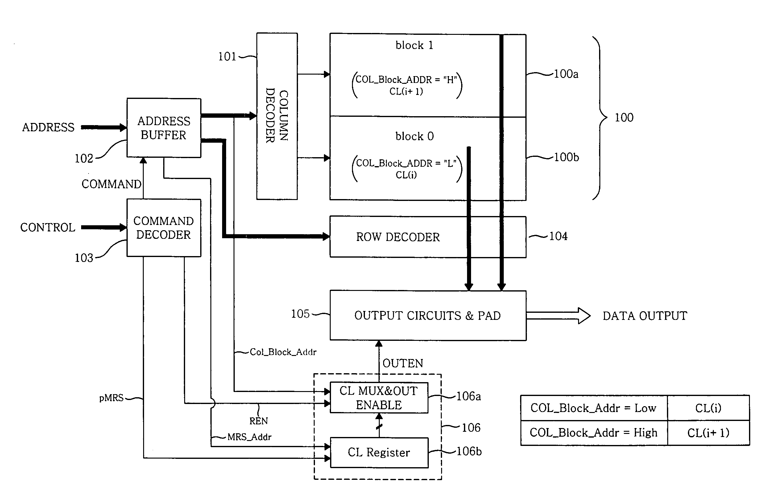
[0085]FIG. 8 illustrates a block diagram of a synchronous memory device according to an embodiment of the present general inventive concept. Referring to FIG. 8, a memory bank 100 includes a memory block_0100b (i.e., a near memory block) and a memory block_1100a (i.e., a far memory block). A column decoder 101 and a row decoder 104 are used to access specific portions of a block within the bank 100 using logic codes. An address buffer 102 receives signals that are addresses of a block to be accessed (e.g., from a read command), and provides the addresses to each of the column decoder 101 and the row decoder 104. In ...


PUM


Abstract

An apparatus and method to delay output of data from different regions of a memory device in response to a read enable signal, the delaying of the output of data is based on the location of the regions of the memory device with respect to an output circuit that receives the data, wherein the different regions of the memory device have different CAS latency values dedicated to each region to set the delay time of each region of the memory device.

Description

CROSS-REFERENCE TO RELATED APPLICATIONS [0001] This application claims the benefit of Korean Patent Application No.10-2005-65437 filed on Jul. 19, 2005, in the Korean Intellectual Property Office, the disclosure of which is incorporated herein in its entirety by reference. BACKGROUND OF THE INVENTION [0002] 1. Field of the Invention [0003] The present general inventive concept relates to semiconductor memory devices, and more particularly, to synchronous memory devices having a block-dedicated programmable latency register. [0004] 2. Description of the Related Art [0005]FIG. 1 is a timing diagram illustrating a read operation of a semiconductor memory device (SDRAM). In FIG. 1, CLK refers to a clock signal, COMMAND in this example refers to a read command, ADDRESS refers to a signal providing instructions to access a column address, and DATA OUTPUT illustrates the output of the memory device at any particular time. Latency generally refers to the time between the start and the compl...

Claims


Application Information

Patent Timeline
Patent Type & Authority Applications(United States)
IPC IPC(8): G11C7/00
CPCG11C7/1045G11C7/1051G11C7/1066G11C11/4096G11C7/22G11C11/4076G11C11/4087G11C7/1069G11C7/10
Inventor PARK, CHUL WOO
Owner SAMSUNG ELECTRONICS CO LTD
Why Eureka
Try Eureka