Circuit substrate and method of manufacturing the same

Active Publication Date: 2007-01-25
SHINKO ELECTRIC IND CO LTD
View PDF8 Cites 19 Cited by
  • Summary
  • Abstract
  • Description
  • Claims
  • Application Information

AI Technical Summary

Benefits of technology

[0014] An object of the present invention is to provide a circuit substrate in which two independent, highly-reliable conducting paths are formed in a through hole of a substrate to enable conduction between the two sides of the substrate without causing any problems, and to provide a method of manufacturing the same.
[0017] Thus, in the present invention, the outer and inner through conducting portions constituting a coaxial structure are formed in one through hole of the semiconductor substrate in a state in which the outer and inner through conducting portions are insulated from each other by the second insulating layer. Accordingly, unlike the prior art, two independent conducting paths which enable conduction between the two sides of the semiconductor substrate can be easily formed without unnecessarily increasing the number of through holes and without limiting a wiring layout.
[0019] By doing so, when the second insulating layer is formed, the second through hole is thereby also formed simultaneously. Accordingly, the step of forming the second through hole becomes unnecessary. Thus, cost can be reduced compared to that of a method in which an opening is formed in an insulating layer using a laser, and it is possible to easily cope with the case where the first through hole becomes smaller.
[0020] As described above, in the present invention, two fine conducting paths can be easily formed in a through hole of a semiconductor substrate without causing any problems.

Problems solved by technology

However, in the prior art, since one conducting path is formed in a through hole of a substrate, the number of through holes becomes large in the case where both sides of the substrate are connected to each other by two independent conducting paths.
Thus, there is a problem that a wiring layout is limited.
However, since this is a method in which conductive components are inserted into a through hole, it is very difficult to apply this method to fine through holes provided in a semiconductor substrate having a reduced thickness.

Method used


Image

  • Circuit substrate and method of manufacturing the same
  • Circuit substrate and method of manufacturing the same
  • Circuit substrate and method of manufacturing the same

Examples


first embodiment

(First Embodiment)

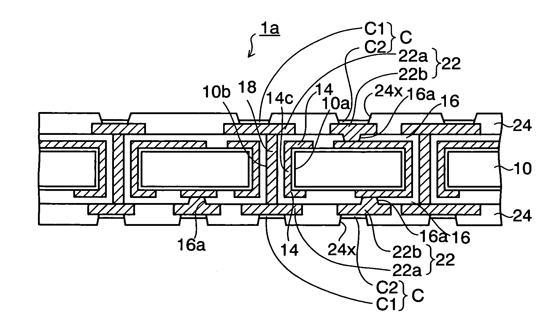
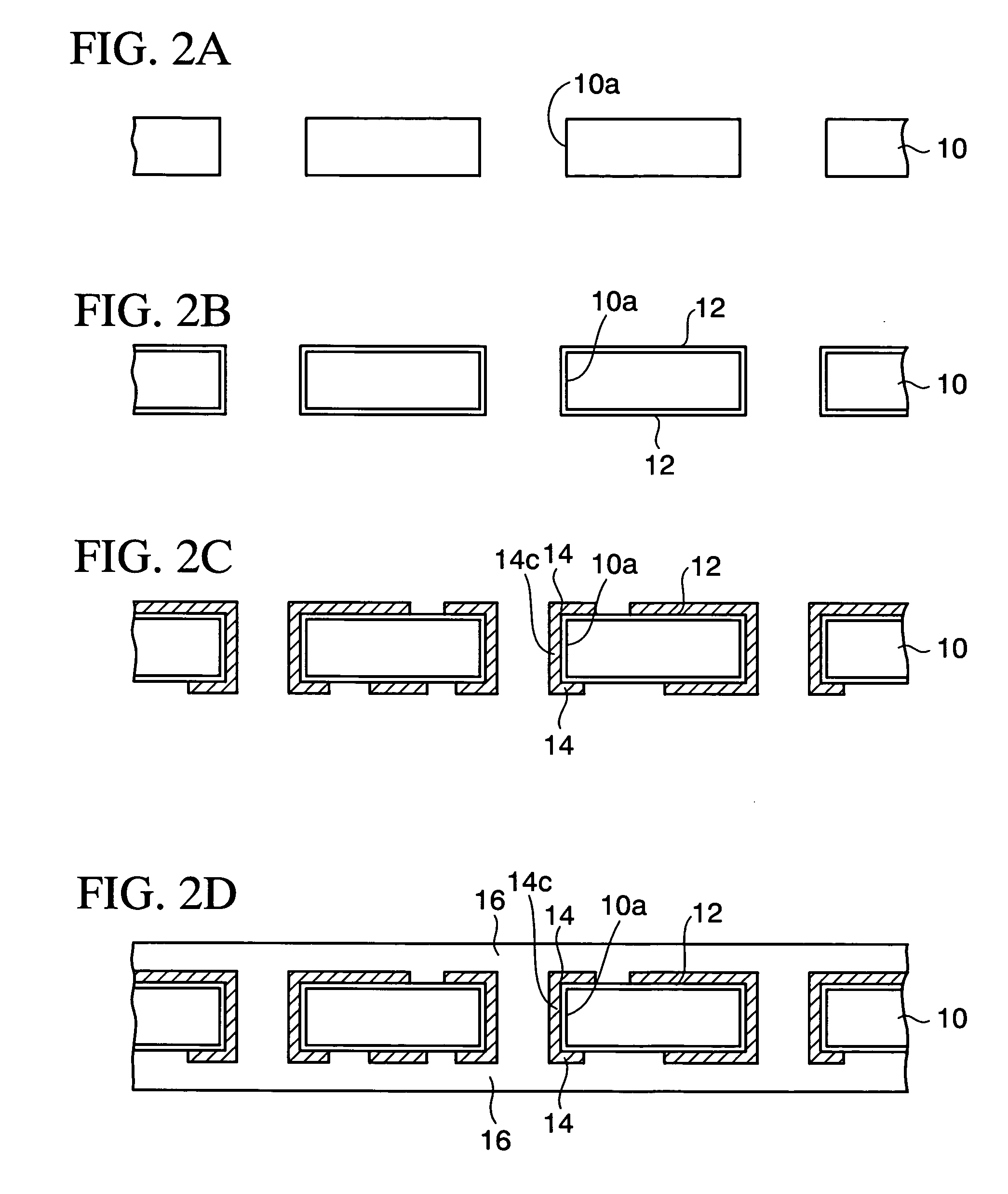
[0028]FIGS. 2A to 2I are cross-sectional views showing a method of manufacturing a circuit substrate of a first embodiment of the present invention. FIG. 3 is a cross-sectional view showing the circuit substrate of the first embodiment. FIGS. 4A to 4D are cross-sectional views showing details of the step of FIG. 2C. FIGS. 5A to 5C are cross-sectional views showing details of the step of FIG. 2F.

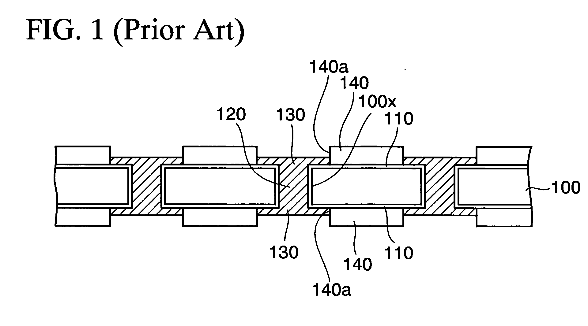
[0029] First, as shown in FIG. 2A, a silicon substrate 10 is prepared as a semiconductor substrate, and first through holes 10a are formed which penetrate the silicon substrate 10 in the thickness direction thereof. As a method of forming the first through holes 10a, a method is employed in which a mask (not shown) having opening portions provided therein is formed on the silicon substrate 10 and in which the silicon substrate 10 is etched by RIE through the opening portions of the mask. In this embodiment, since the silicon substrate 10 thickness of which is reduced to 50 ...

second embodiment

(Second Embodiment)

[0049]FIGS. 6A to 6G are cross-sectional views showing a method of manufacturing a circuit substrate of a second embodiment of the present invention.

[0050] The second embodiment differs from the first embodiment in that the second insulating layer 16 which covers the outer through conducting portions 14c on the inner surfaces of the first through holes 10a is formed by CVD. In the second embodiment, steps similar to those of the first embodiment will not be described in detail.

[0051] First, as shown in FIG. 6A, the same structure as in FIG. 2C is formed by a method similar to that of the first embodiment. That is, the first wiring layers 14 connected to each other via the outer through conducting portions 14c on the inner surfaces of the first through holes 10a are respectively formed on both sides of the silicon substrate 10. Then, as shown in FIG. 6B, the second insulating layer 16 is formed on the first wiring layers 14 on both sides of the silicon substrate ...


PUM

PropertyMeasurementUnit
Temperatureaaaaaaaaaa
Thicknessaaaaaaaaaa
Diameteraaaaaaaaaa

Abstract

In a method of manufacturing a circuit substrate of the present invention, a first through hole is formed in a semiconductor substrate and a first insulating layer is formed on the entire surface of the semiconductor substrate, and then first wiring layers connected to each other via an outer through conducting portion provided on the inner surface of the first through hole are formed on both sides of the semiconductor substrate, and then a second insulating layer is formed which covers the first wiring layers on both sides of the semiconductor substrate and the outer through conducting portion on the inner surface of the first through hole, the second insulating layer has a structure in which a second through hole is provided in a central portion of the first through hole, and then second wiring layers connected to each other via an inner through conducting portion provided in the second through hole are formed on the second insulating layer on both sides of the semiconductor substrate.

Description

CROSS-REFERENCE TO RELATED APPLICATIONS [0001] This application is based on and claims priority of Japanese Patent Application No. 2005-208080 filed on Jul. 19, 2005, the entire contents of which are incorporated herein by reference. BACKGROUND OF THE INVENTION [0002] 1. Field of the Invention [0003] The present invention relates to a circuit substrate and a method of manufacturing the same. More specifically, the present invention relates to a circuit substrate having a structure which enables conduction between the two sides of a substrate via a conductor in a through hole provided in the substrate, and relates to a method of manufacturing the same. [0004]2. Description of the Related Art [0005] Heretofore, there are circuit substrates having a structure in which wiring layers formed on both sides of a silicon substrate are connected to each other through conductors provided in through holes of the silicon substrate. [0006] A method of manufacturing such a circuit substrate will b...

Claims


Application Information

Patent Timeline
IPC IPC(8): H01L21/4763H01L23/52H01L23/48H01L29/40
CPCH01L21/486Y10T29/49123H01L23/49822H01L23/49827H05K1/0306H05K1/115H05K3/4608H05K2201/09536H05K2201/09809H01L2924/0002H01L23/147Y10T29/49155Y10T29/49165H01L2924/00
Inventor HIGASHI, MITSUTOSHI
Owner SHINKO ELECTRIC IND CO LTD
Why Eureka
Try Eureka