

Laser processing apparatus
a technology of laser processing and workpiece, which is applied in the field of laser processing equipment, can solve the problems of deteriorating chip quality and damaging the device, and achieve the effect of softening the processing area of the workpi
- Summary
- Abstract
- Description
- Claims
- Application Information
AI Technical Summary
Benefits of technology
Problems solved by technology
Method used
Image

Examples
Embodiment Construction
[0021] Preferred embodiments of a laser processing apparatus constituted in accordance with the present invention will now be described in detail by reference to the accompanying drawings.
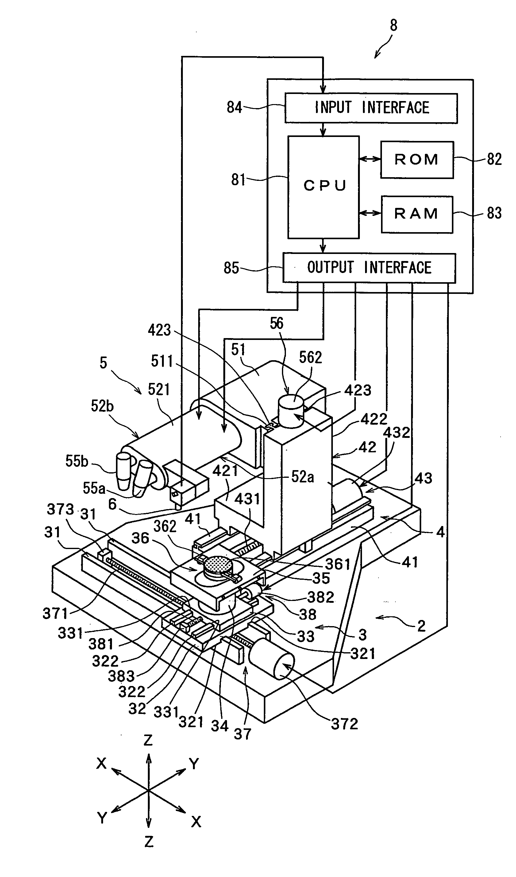
[0022]FIG. 1 shows a perspective view of the laser processing apparatus constituted in accordance with the present invention. The laser processing apparatus shown in FIG. 1 is equipped with a stationary pedestal 2, a chuck table mechanism 3, disposed on the stationary pedestal to be movable in a processing feed direction indicated by an arrow X, for holding a workpiece, a laser beam irradiation unit support mechanism 4 disposed on the stationary pedestal 2 to be movable in an indexing feed direction indicated by an arrow Y which is perpendicular to the direction indicated by the arrow X, and a laser beam irradiation unit 5 disposed on the laser beam irradiation unit support mechanism 4 to be movable in a direction indicated by an arrow Z.
[0023] The chuck table mechanism 3 is furnished with a pair...
PUM
| Property | Measurement | Unit |
|---|---|---|
| Width | aaaaa | aaaaa |
| Frequency | aaaaa | aaaaa |
| Wavelength | aaaaa | aaaaa |
Abstract
Description
Claims
Application Information