Voltage generating circuit, semiconductor memory device comprising the same, and voltage generating method

a voltage generation circuit and semiconductor technology, applied in the direction of information storage, static storage, digital storage, etc., can solve the problems of significantly reducing voltage generation efficiency and difficult to maximize the transfer characteristics of the transfer transistor

Active Publication Date: 2007-02-01
SAMSUNG ELECTRONICS CO LTD
View PDF6 Cites 50 Cited by
  • Summary
  • Abstract
  • Description
  • Claims
  • Application Information

AI Technical Summary

Problems solved by technology

However, when the boosted voltage at the boosting node is output, the voltage level at a gate node of a transfer transistor is smaller than the boosted voltage level at the boosting node, which makes it difficult to maximize the transfer characteristics of the transfer transistor.
This phenomenon becomes worse as Vcc decreases or as a target Vpp increases, thereby significantly reducing voltage generation efficiency.

Method used


Image

  • Voltage generating circuit, semiconductor memory device comprising the same, and voltage generating method
  • Voltage generating circuit, semiconductor memory device comprising the same, and voltage generating method
  • Voltage generating circuit, semiconductor memory device comprising the same, and voltage generating method

Examples


Embodiment Construction

[0021] Hereinafter, exemplary embodiments of the present invention will be described in detail with reference to the attached drawings. Like reference numerals in the drawings denote like elements.

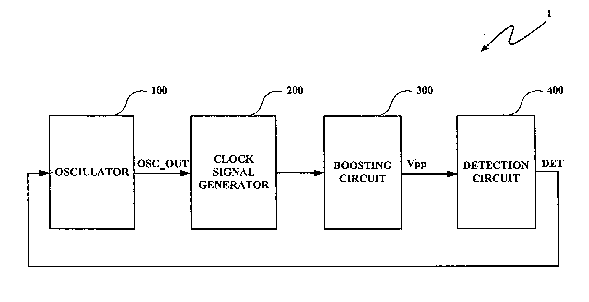
[0022]FIG. 1 is a block diagram illustrating a voltage generating circuit 1 for a semiconductor memory device according to an exemplary embodiment of the present invention.

[0023] Referring to FIG. 1, the voltage generating circuit includes an oscillator 100, a clock signal generator 200, a boosting circuit 300, and a detection circuit 400.

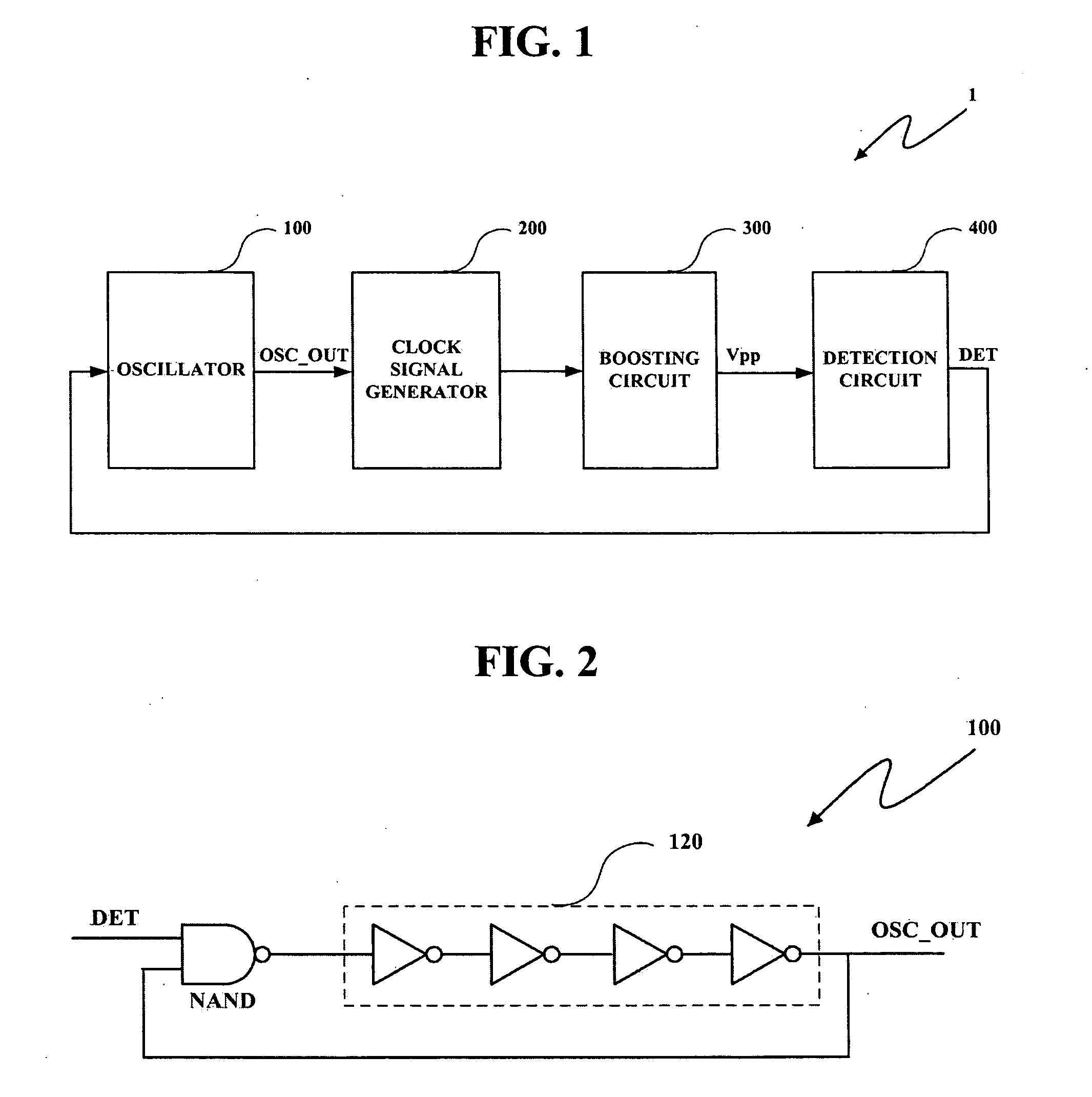
[0024] The oscillator 100 generates an oscillator output signal OSC_OUT for triggering the operation of the clock signal generator 200, in response to a detection signal DET. The oscillator 100 may be implemented by a ring oscillator.

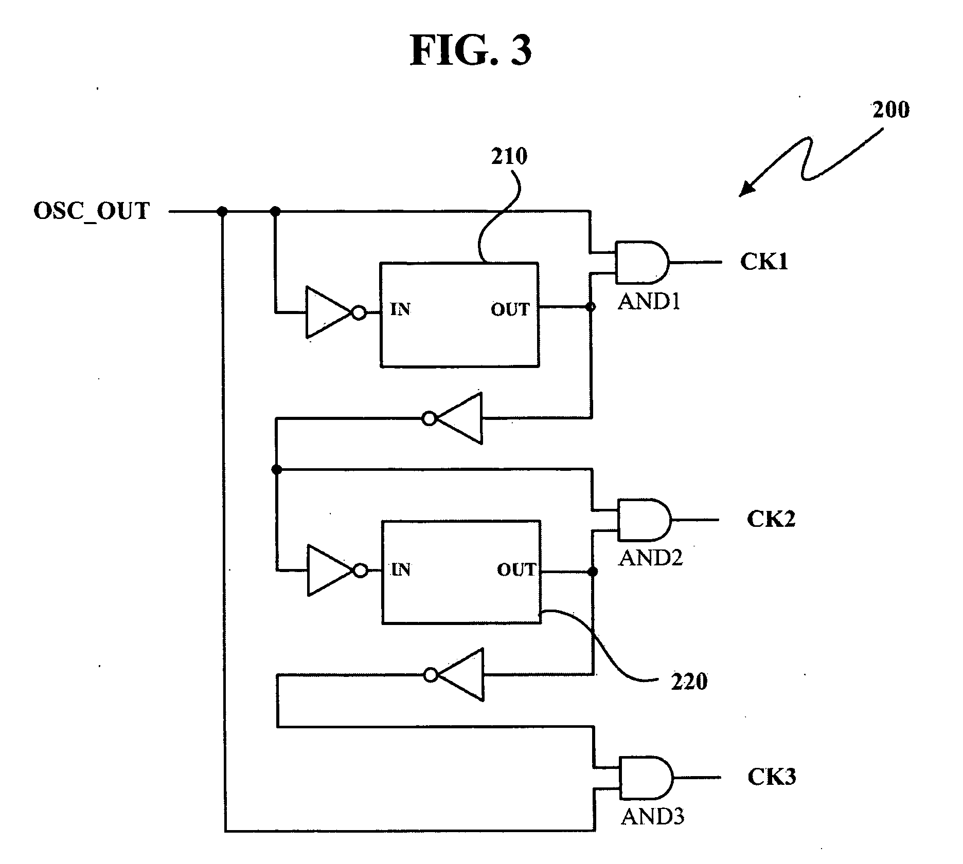
[0025] In response to the oscillator output signal OSC_OUT, the clock signal generator 200 generates signals for controlling the operation of the boosting circuit 300. The signals may include multiple boosting signals CK1...


PUM


Abstract

A voltage generating circuit for a semiconductor memory device. The voltage generating circuit includes a multi-boosting unit for stepping up a power supply voltage, a transfer transistor connected to a final boosting node of the multi-boosting unit and an output node, and a charge-sharing element, electrically connected to the final boosting node and a gate node of the transfer transistor, enabled during at least a part of the period the power supply voltage is stepped-up by the multi-boosting unit and performing charge sharing between the final boosting node and the gate node of the transfer transistor.

Description

CROSS-REFERENCE TO RELATED PATENT APPLICATION [0001] This application claims priority to Korean Patent Application No. 2005-0068996, filed on Jul. 28, 2005, in the Korean Intellectual Property Office, the disclosure of which is incorporated by reference herein. BACKGROUND OF THE INVENTION [0002] 1. Technical Field [0003] The present disclosure relates to a voltage generating circuit, a semiconductor memory device comprising the same, and a voltage generating method. More particularly, the present invention relates to a voltage generating circuit, a semiconductor memory device comprising the same, and a voltage generating method, which can efficiently drive low voltages. [0004] 2. Discussion of the Related Art [0005] Semiconductor memory devices utilize a voltage generating circuit according to the operational needs of their internal circuits. In particular, a boosted voltage (Vpp), which is higher than a power supply voltage (Vcc), is generally utilized in semiconductor memory devic...

Claims


Application Information

Patent Timeline
Patent Type & Authority Applications(United States)
IPC IPC(8): G11C7/00
CPCG11C5/145G11C5/14
Inventor KIM, JUN-HYUNGBAE, WON-ILJANG, SEONG-JIN
Owner SAMSUNG ELECTRONICS CO LTD
Why Eureka
Try Eureka