Printed circuit board and soldering method and apparatus

Inactive Publication Date: 2007-02-08
PANASONIC EV ENERGY CO LTD
View PDF5 Cites 22 Cited by
  • Summary
  • Abstract
  • Description
  • Claims
  • Application Information

AI Technical Summary

Benefits of technology

[0009] An object of the invention is to solve these problems encountered by the conventional techniques and to provide a printed circuit board and a method and apparatus for dip so

Problems solved by technology

The reduced temperature also causes a decrease in solder flowability, which leads to air entrapment.
Furthermore, the temperature difference between the upper and lower parts of solder inside the thr

Method used


Image

  • Printed circuit board and soldering method and apparatus
  • Printed circuit board and soldering method and apparatus
  • Printed circuit board and soldering method and apparatus

Examples


first embodiment

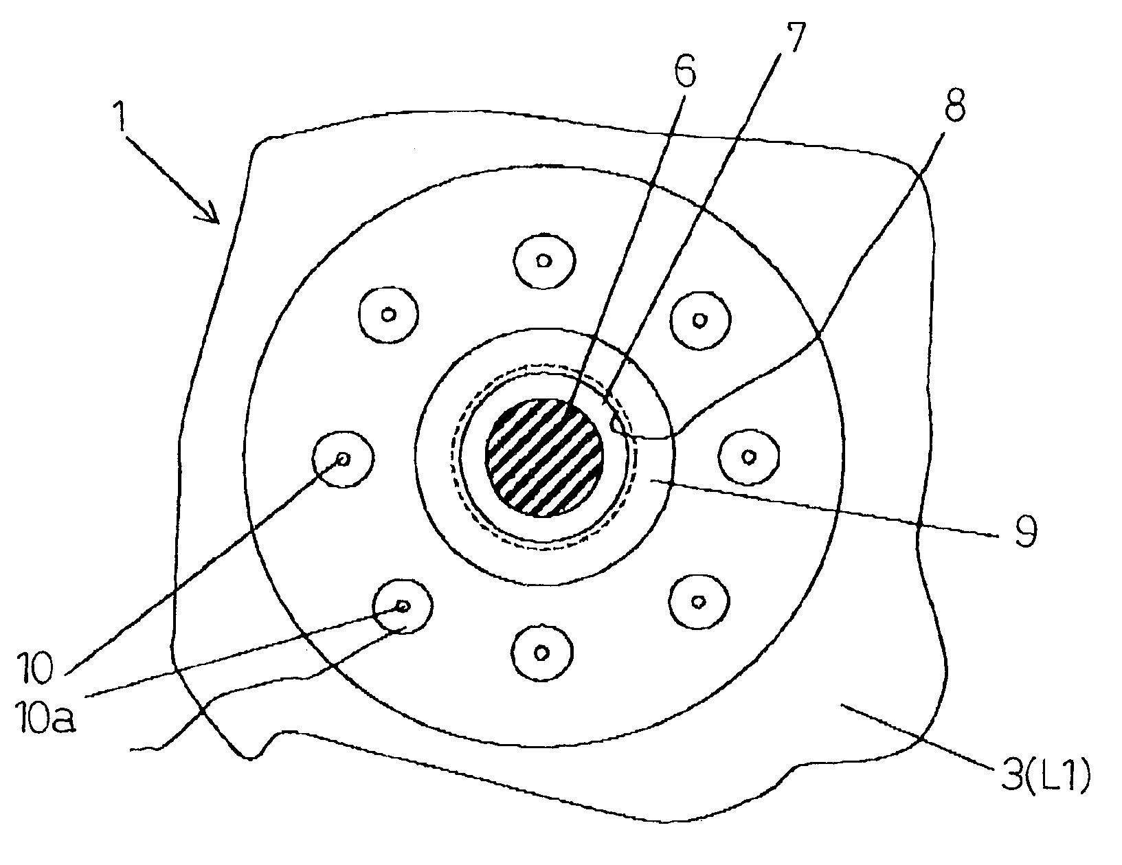
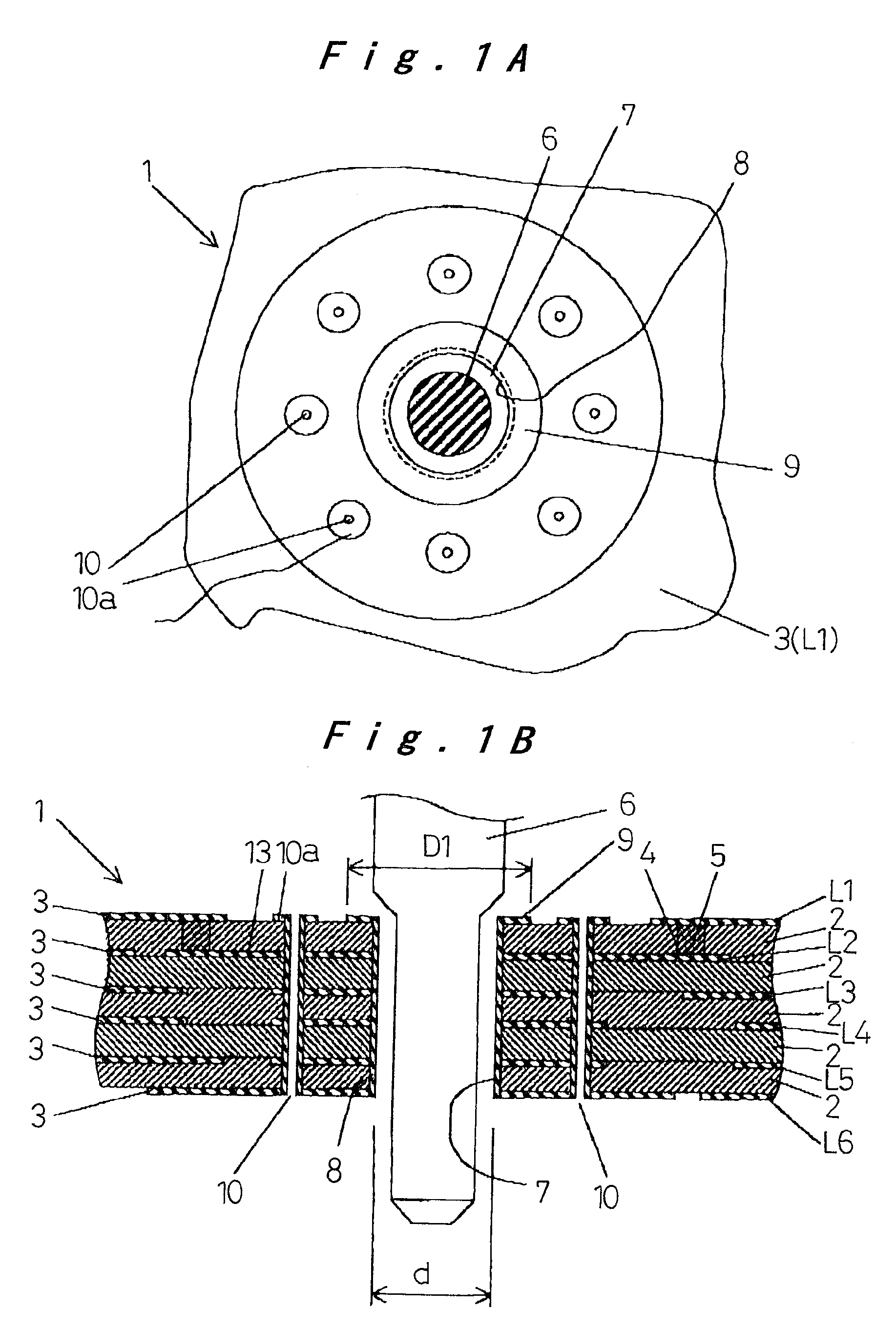
[0030] A first embodiment will be described with reference to FIG. 1A, FIG. 1B, and FIG. 2. FIG. 1A and FIG. 1B show a multilayer printed circuit board 1 made up of five laminated insulating resin plates 2 such as glass epoxy resin. Six layers of metal foil patterns 3 such as copper foil patterns are formed as required on the front and back surfaces and in between the resin plates, denoted at L1 to L6 from the front side. These patterns 3 are connected to each other through conductive material 5 filled in holes 4 drilled in any of the insulating resin plates 2 so as to construct a three-dimensional, high-density wiring pattern.

[0031] The printed circuit board 1 includes a through hole 7 extending from the front surface to the back surface at an appropriate location of a power supply terminal pattern or ground pattern that stretches continuously over a wide area in the front metal foil pattern 3 (L1). A lead 6 of an electronic component is inserted through the hole 7 and soldered. A...

second embodiment

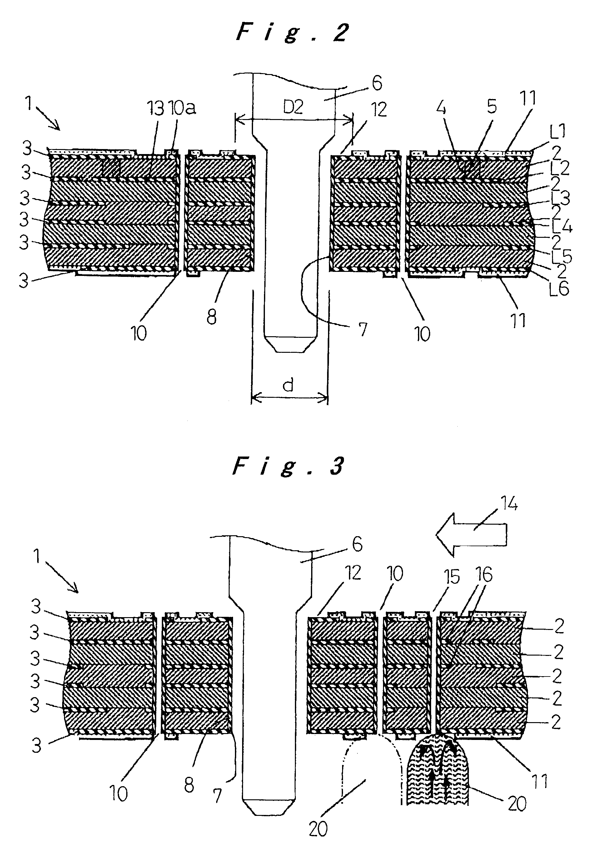
[0037] Next, a second embodiment will be described with reference to FIG. 3. Since many of the components are the same as those previously described, like components will have the same reference numerals and only the differences will be described.

[0038] In this embodiment, a via hole 15 is provided in addition to the via holes 10 on the side opposite from the direction of movement 14 of the board 1 indicated by the white arrow during the dip soldering operation. At least one or more upper layers of metal foil patterns 3 apart from the surface pattern, in the illustrated example the second and third layers of patterns L2 and L3, include connection patterns 16 to connect the via hole 15 with the tubular metal foil 8, so as to conduct heat of the solder to the through hole 7 through the via hole 15.

[0039] With this configuration, when the printed circuit board 1 undergoes the dip soldering operation in which it is moved above a dipping section 20 where molten solder is ejected upward...

third embodiment

[0040] Next, a third embodiment will be described with reference to FIG. 4.

[0041] In this embodiment, the metal foil patterns 3 (L1 and L6) on the front surface and the back surface of the printed circuit board 1 are connected through via holes 17, on the outer side of the region where the insulating resin plate 2 is exposed around the through hole 7 on the surface of the board 1.

[0042] With this configuration, the high frequency impedance is lowered by connecting the metal foil patterns 3 (L1 and L6) on the front surface and the back surface by the solder filled in the via holes 17. This compensates for any decrease in the EMC effect caused by the absence of the metal foil pattern 3 (L1) over a relatively large area around the through hole 7 on the surface of the printed circuit board 1 and the lack of direct connection between the pattern 3 (L1) and the tubular metal foil 8 of the through hole 7.


PUM

PropertyMeasurementUnit
Timeaaaaaaaaaa
Speedaaaaaaaaaa
Radiusaaaaaaaaaa

Abstract

A printed circuit board suitable for dip soldering of component leads in through holes using lead free solder. The printed circuit board includes a plurality of via holes arranged around each through hole in which a component lead is inserted, whereby solder wicking up into the through hole is enhanced and air entrapment is prevented during the dip soldering operation, and heat fatigue resistance of solder joints is improved.

Description

[0001] The present disclosure relates to subject matter contained in priority Japanese Patent Application No. 2005-227876, filed on Aug. 5, 2005, the contents of which is herein expressly incorporated by reference in its entirety. BACKGROUND OF THE INVENTION [0002] 1. Field of the Invention [0003] The present invention relates to a printed circuit board suitable for dip soldering of component leads in through holes of the printed circuit board using lead free solder, and a method and apparatus for dip soldering. [0004] 2. Description of the Related Art [0005] Dip soldering that uses Sn—Pb eutectic solder is a common method of soldering component leads in through holes of printed circuit boards. A power supply terminal pattern or ground pattern on the surface of a printed circuit board consisting of copper foil 31 usually stretches over a wide area in a continuous manner as shown in FIG. 6A and FIG. 6B. A through hole 33 with a copper foil 34 on its inner surface is provided in a por...

Claims


Application Information

Patent Timeline
IPC IPC(8): H05K1/11H05K3/34H05K3/42
CPCB23K1/085H05K1/116H05K3/3447H05K3/3468H05K3/3494H05K3/429Y10T29/49165H05K2201/09627H05K2201/0979H05K2201/09809H05K2203/0557H05K2203/304Y10T29/49144H05K2201/09618
Inventor NAKAO, YOSHITADATSUTSUMI, MASATERUFUJIKAWA, TAKAYUKI
Owner PANASONIC EV ENERGY CO LTD
Why Eureka
Try Eureka