Bipolar junction transistor and method of fabricating the same

a bipolar junction transistor and transistor technology, applied in the field of semiconductor devices, can solve the problems of low current gain of bipolar junction transistors and serious reverse junction leakage, and achieve the effect of reducing reverse junction leakage curren

Active Publication Date: 2007-02-15
UNITED MICROELECTRONICS CORP
View PDF6 Cites 7 Cited by
  • Summary
  • Abstract
  • Description
  • Claims
  • Application Information

AI Technical Summary

Benefits of technology

[0005] Accordingly, at least one objective of the present invention is to provide a bipolar junction transistor and method of fabricating thereof that can reduce the reverse junction leakage current of the device.

Problems solved by technology

Since the p-type base contacts with the n-type collector directly, reverse junction leakage is a serious problem.
Moreover the current gain of the bipolar junction transistor is low.

Method used


Image

  • Bipolar junction transistor and method of fabricating the same
  • Bipolar junction transistor and method of fabricating the same
  • Bipolar junction transistor and method of fabricating the same

Examples


Embodiment Construction

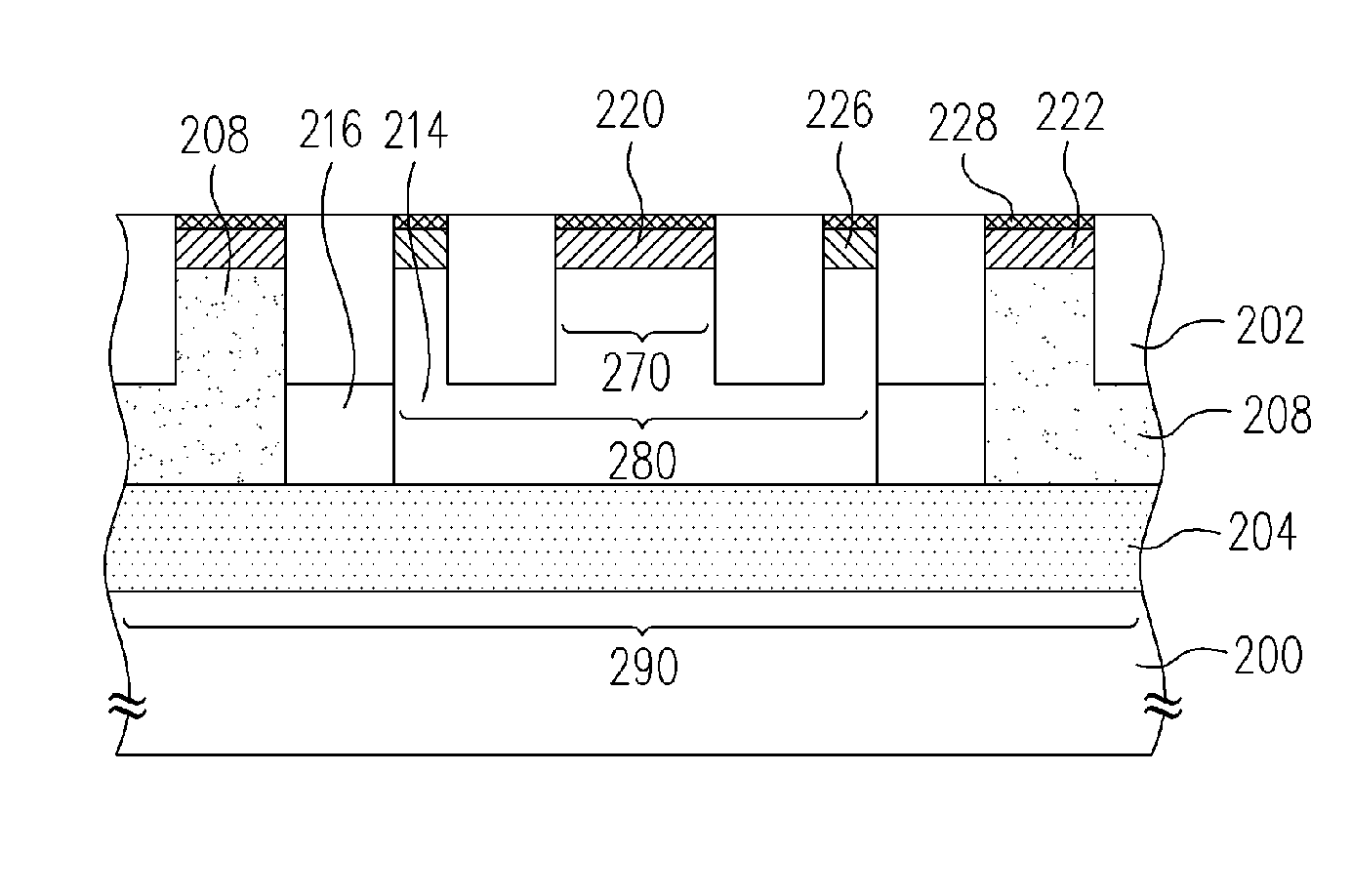
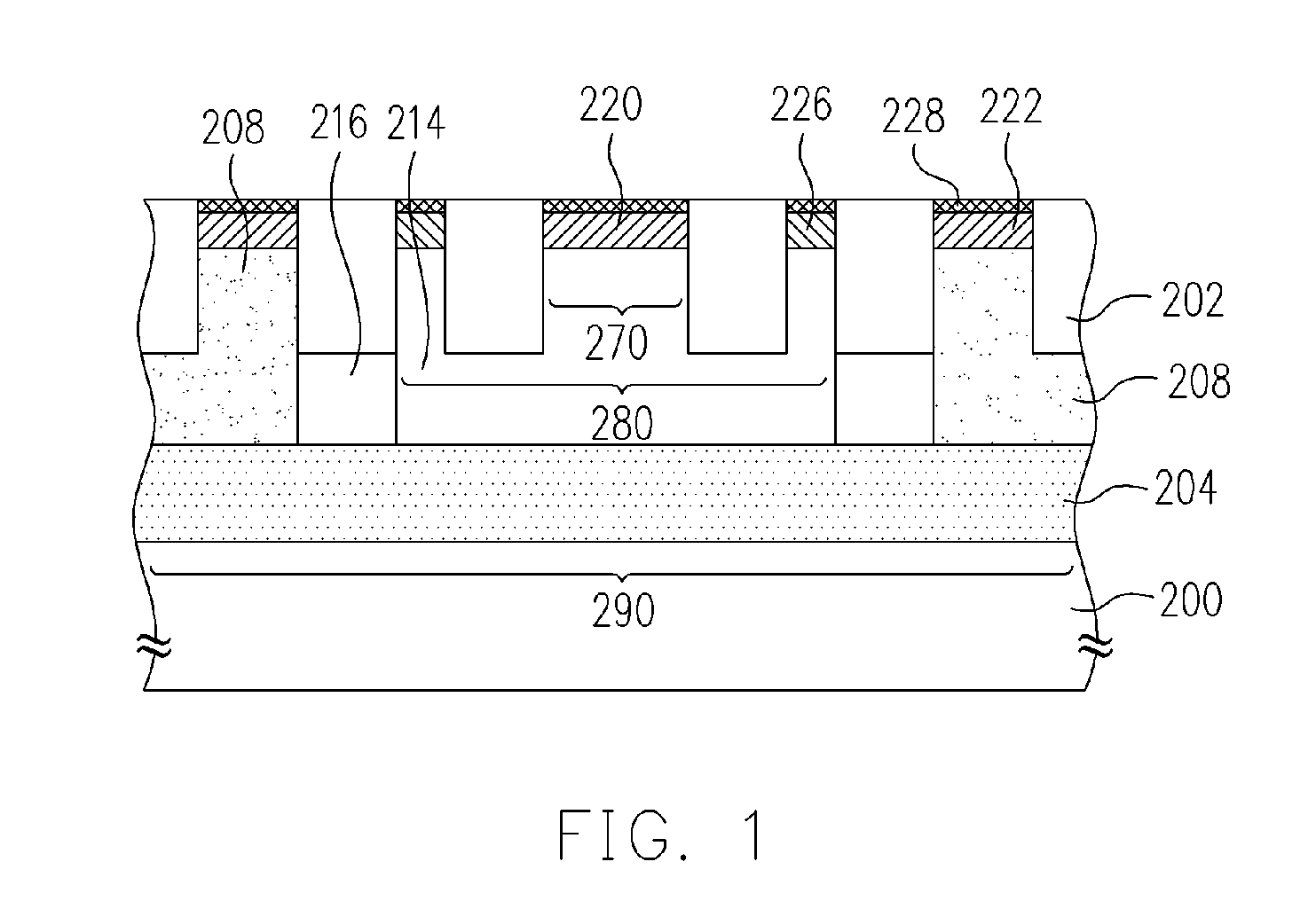
[0027] Reference will now be made in detail to the present preferred embodiments of the invention, examples of which are illustrated in the accompanying drawings. Wherever possible, the same reference numbers are used in the drawings and the description to refer to the same or like parts.

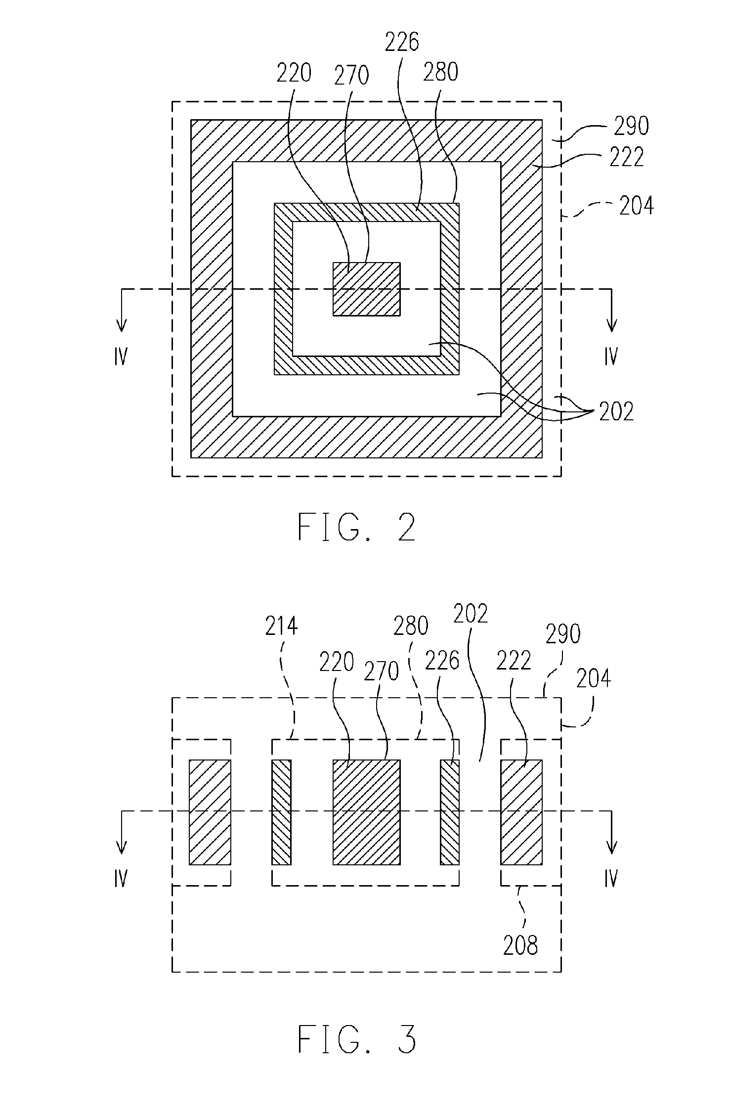
[0028]FIG. 1 is a schematic cross-sectional view of a bipolar junction transistor according to the present invention. FIG. 2 is a top view of the bipolar junction transistor in FIG. 1 without showing a silicide layer. FIG. 3 is a top view of another bipolar junction transistor in FIG. 1 without showing a silicide layer. In the following, an n-p-n bipolar junction transistor is used to simplify explanations. This should by no means limit the present invention as such. The method in the present invention applies equally to a p-n-p bipolar junction transistor.

[0029] As shown in FIGS. 1 and 2, the bipolar junction transistor of the present invention comprises a buffer region 216 that isolates a p-type...


PUM


Abstract

A bipolar junction transistor is provided. A p-type well region surrounds an n-type emitter and connects with the bottom of the emitter to serve as a base. A p-type base pick-up region connects with the base and surrounds the emitter. An n-type deep well, connected to the bottom of the base and the bottom of the n-type well, is used as a collector. The n-type well surrounds the base and connects with the n-type deep well. An n-type collector pick-up region connects with the n-type well and surrounds the base. An isolation structure is disposed between the emitter and the base and between a portion of the base and a portion of the n-type well. A buffer region is disposed under a portion of the isolation structure. Furthermore, the buffer region together with a portion of the isolation structure isolates the p-type base from the n-type well.

Description

BACKGROUND OF THE INVENTION [0001] 1. Field of the Invention [0002] The present invention relates to a semiconductor device and method of fabricating the same. More particularly, the present invention relates to a bipolar junction transistor structure and method of fabricating the same. [0003] 2. Description of the Related Art [0004] In the modern integrated circuit design, bipolar junction transistors are often used in high voltage, high power or high frequency sections as well as places requiring quick switching. Bipolar junction transistors includes p-n-p junction type and n-p-n junction type. The n-type collector of a typical n-p-n bipolar junction transistor is an n-type well formed in a p-type substrate. The p-type base is a p-type well formed within the n-type well. The n-type emitter is an n-doped region within the p-type well. Since the p-type base contacts with the n-type collector directly, reverse junction leakage is a serious problem. Moreover the current gain of the bi...

Claims


Application Information

Patent Timeline
Patent Type & Authority Applications(United States)
IPC IPC(8): H01L31/00
CPCH01L29/0821H01L29/732H01L29/66272
Inventor TSAI, MINGSHANG
Owner UNITED MICROELECTRONICS CORP
Why Eureka
Try Eureka